We might wish that all our design automation needs could be handled by pre-packaged vendor tool features available at the push of a button, but that never was and never will be the case. In the language of crass commercialism, there may be no broad market for those features, even though you consider that analysis absolutely essential.
Much of the analysis of this type is motivated by insufficient capabilities to do comprehensive checks through simulation. This is particularly the case in top-level checking on very large designs, but I have seen examples of in-house automation starting as small (ha-ha) as 20M gates. Typical questions include whether all blocks are hooked up correctly (per spec requirements) or more quickly localizing latency or coverage problems in a design.
Connectivity checks are a good example of this class. For connectivity between two instances of two specific IPs, you might have a requirement that say ports beginning with “a” cannot connect to ports beginning with “q”. This kind of checking can get progressively more elaborate. A clock pin must be driven by a clock source in the appropriate domain; it also can only be gated by a signal from an appropriate source. Reset pins have similar requirements and must be grouped accordingly into reset domains.
This concept need not be limited to static and netlist-specific checks. You might also want to look at power intent, simulation data, performance data and formal analysis. And you might not just want to do checking/analysis – you might also want that analysis to drive design modification.
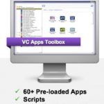
Building these kinds of capabilities starts with user-extensibility to core tools. I’m pretty familiar with this concept from my Atrenta days – we built extensibility into SpyGlass and other tools through Tcl, Perl and C interfaces. But I’m in awe of what you can do through the Synopsys VC Apps. These give you a unified interface to data for the design, simulation, coverage, power intent, formal analysis and more.
VC Apps is a programming interface, through Tcl or C, to customize Verdi. And since Verdi is the integrated debug platform in Verification Compiler, that means you can get to anything Verdi can get to. Several examples were presented:
- General connectivity checking, also graphing completion of connectivity by different classes (I would guess clock, reset, communication, that sort of thing)
- Looking for high latency on reads and writes to memory, then color-coding read/write-enables in the simulation waveform corresponding to those cases
- Generating specialized power instrumentation rules by looking at both the design and power intent
Why support both Tcl and C? Good question. Tcl is great for quick one-off checks, and maybe even long term checks which you’ll make part of your regression. And Synopsys Tcl provides a lot of nice grouping and filtering features which otherwise you’d have to write yourself. But if you need to write computationally intensive applications and you’re comfortable in C or C++, you may find the C API is faster. Either way, you can access a lot of capability.
You can learn more about VC Apps HERE.