The move towards 5G networks with demands for decreased latency ( 100 devices/m[SUP]2[/SUP]), and the desire to flexibly configure and integrate mobile, fixed, optical and satellite telecommunications is putting tremendous pressure on the design of next generation telecom equipment. Silicon photonics promises to be the most viable solution to the growing need for communication networks with increased flexibility, processing capacity and bandwidth density while at the same time delivering reduced cost, power consumption and footprint.
A team from Ericsson Research in Pisa, Italy, captured their thoughts on what next generation optical transport networks will look like in chapter 15 of the recently published book, Silicon Photonics III. Their opinion is that next generation optical networks must be capable of performing dynamic rearrangement of bandwidth while optimizing resource utilization and power consumption. Furthermore, they believe this will be enabled by highly flexible transport nodes in conjunction with an intelligent control and management plane based on software-defined networking (SDN). A high level view of the current optical transport network is depicted in Fig 15.12 and is divided into four segments.
[LIST=1]
The higher volumes of switches that promise to drive integrated silicon photonics are in the metro-aggregation and access transport nodes. To support 5G and associated multi-directional video traffic that is coming, an all-optical switching layer must be implemented based on scalable, high capacity and transparent switching subsystems. At the heart of each node is a multi-directional ROADM (re-configurable optical add/drop multiplexer) whose function is to add and/or drop a certain number of WDM channels carrying local traffic from data centers or client switching equipment to/from the main networks. Highly flexible optical switching nodes are needed with the following characteristics:
- Full remote re-configuration without the need for any manual intervention
- Automated control and light-path set-up
- Capability of re-configuring the light-paths in sub-milliseconds for on-the-fly connection restoration
Conventional ROADM switches only provide flexibility to reconfigure input/output communications of the switch in the main network. However, the add/drop functionality that enables connections from nodes to local resources are currently rigidly assigned and can only be changed by manually re-wiring the connections. Additionally, these wavelength selective switches (WSS) are currently made using discreet high-performance free-space optics that are both costly and bulky. These existing switches are too expensive to move into the higher-volume access and metro-aggregation networks and represent new opportunity for integrated silicon photonic solutions.
Next generation ROADMs built using integrated silicon photonics will have the ability to not only be re-configurable at the local level but they will also be colorless, directionless and contention-less (CDC). With these new switches it will be possible through SDNs, without any manual intervention, to change the configuration of add/drop wavelength channels to/from any direction (direction-less), independent of the transponder wavelengths (color-less), while allowing multiple signals with the same wavelength to be handled by the same add/drop structure (contention-less). Silicon photonic-based CDC-ROADMs will give the operator the ability to optimize resource utilization, reconfigure network bandwidth according to the variation of traffic patterns depending on time of day and day of week usage and support rerouting functions in case of network faults in a cost effective way. The CDC-ROADMs will make use of new blocks in the Add/Drop sections of the switch called transponder aggregators (TPAs). TPAs will distribute and select the multiplexed signals before filtering the individual channels by the use of tunable filters and add flexibility to the exact point of the optical node where the older ROADMs lacked it.
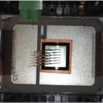
One instance of this new architecture is being put into reality through a project known as IRIS, funded by the European Union’s Seventh Framework Programme. IRIS will implement a complete TPA optical switching subsystem using a monolithic integration of all functions on one Photonic System-on-Chip (PSoC) IC.
Make no mistake, integrated silicon photonics is coming. It’s not a question of “if” but only a question of “when”. The drive towards bidirectional on-demand video and the push to 5G networks with millions of mobile devices and sensors will be the forcing function that brings silicon photonics into the volumes that will get the attention of every foundry.