I recently attended the IoT Developers Conference in Santa Clara, CA. There were clearly two major themes in the talks – security and low power. The volume market in IoT is in the edge node devices. These devices have two important characteristics. They acquire data which needs to be transmitted and they typically are battery-driven or even harvest their own energy. The need for security is clear if the data is sensitive (e.g., vehicle to vehicle communications, medical information, etc.) though not all applications require much security. The need for low power is also obvious for mobile or remote devices which are not plugged into a power outlet.
A common paradigm for these edge node devices is to collect data through their sensors, store it, and then send it in packets either on demand or at some regular interval to a hub device. Of course there may also be a need for code storage, error logging, and still other storage requirements. Clearly these devices will need access to non-volatile memory. The catch is to use a memory device that also doesn’t eat up the entire power budget. Calls for such a solution, a low power non-volatile/flash memory device, have come from such industry leaders as ARM (ARM CEO Simon Segars quoted in EETimes) and Freescale (White Paper: What the Internet of Things (IoT) Needs to Become a Reality) .
Adesto Technologies recently introduced its Ultra-Low Power Moneta™ Non-volatile Serial Memory (RM3000). This new product would seem to dramatically improve the situation for IoT system designers. The RM3000 series makes use of Adesto’s conductive bridging RAM (CBRAM) technology. They claim several advantages from using this technology amongst them, unlike flash memory there is no pre-erase requirement, it has much faster write operations (I saw a demo of this at IoT Dev Con), and it uses a much lower write voltages. Simplifying this it is faster and cheaper on the energy budget.
This technology will start shipping as a packaged part in July 2016 in four densities – 32Kbit, 64Kbit, 128Kbit, and 256Kbit. Of course with my semiconductor IP background I had to ask if this would be coming in an IP form as well. Unfortunately, that is out on the more distant horizon. We need to keep in mind that these resistive RAMs require two extra masks which would complicate the delivery of such an IP. However, an aggressive fab might want to help accelerate the availability of this IP in its production processes. That might give significant advantage over their competition when it comes to an IoT offering.
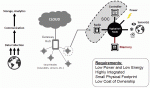
By now you must be wondering… how low-power is it? Really, really low. Here is what Adesto published with the new product announcement (Click on the picture below to enlarge it):
The range of applications enabled by this technology is large but certainly would include a large range of medical devices, environment and security monitoring devices, data logging applications, and probably any device using harvested energy. In fact, I think the ultra-low power level made possible by these devices will enable applications we have not yet thought of, and that is really exciting. For emphasis, the ultra-deep power down state can go as low as 0.05 µW, with read power at 10 µW, and write power at 7.6 µW – that is quite low.
Randy Smith is an advisor at Brown Venture Associates (BVA). Randy and BVA are experienced masters of team building. As a former EDA and semiconductor IP executive, Randy has repeatedly built winning teams. BVA has been doing the same for more than 20 years while building a proprietary recruiting methodology that is geared for the modern recruiting environment. BVA also has invested in 50+ companies with 20+ liquidity events – the teams they build, win.