In the largest and fastest growing categories in electronics – mobile, IoT and automotive – analog is playing an increasingly important role. It’s important in delivering high integrity power and critical signals to the design though LDO regulators and PLLs, in managing high speed interfaces like DDR and SERDES, in interfacing to sensors and in the RF section of communications. And of course memories are analog at heart.
Analog design has an understandable reputation as a black art but analysis and the correct operation of those functions in larger integrations must be precise. This is particularly important around power integrity, noise analysis, EM, ESD and thermal analysis. All of these have to be analyzed in the same level of detail as applied to digital sections of a design. But in this case, analysis must be applied to transistor-level models and their physical implementation.
Unsurprisingly, many potential problems arise because an analog block doesn’t operate in isolation. An LDO regulator needs to manage potential noise at the input in automotive applications for example and it needs to provide a sufficiently steady output under varying load conditions (power domain switching can alter load significantly). You also need to ensure noise coupling through the substrate to sensitive circuits is mitigated. In chip-to-chip communication, the correct function of a SERDES block could be completely undermined by noise, either in the power supply or through the substrate.
EM and thermal problems (thanks to FinFET self-heating) have been published for PLLs at advanced nodes and EM will often be a concern on large drivers and level-shifters. And surprise, surprise, ESD and latchup are concerns around touch-based controls (who wants to wear anti-static clothing to use a touch-screen?). Analyzing ESD becomes particularly complex in the presence of multiple power domains where there are many possible ESD paths.
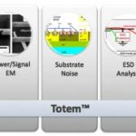
If you’re a digital designer, all these problems should sound familiar and you already know that the gold-standard for analysis and signoff in your domain is Ansys RedHawk. What you may not know is that Ansys has another product, Totem, which provides similar capabilities for analyzing transistor-level designs – which is exactly what you need for analog/full custom applications. And Totem has the same foundry level of support as RedHawk. So can do static IR drop checks, dynamic noise checks, current density and thermal checks and you can check guard-ring robustness as a part of your ESD and latchup signoff.
Totem does its own power and ground RLC extraction and substrate RC extraction. This extraction is not as simple as building lumped models – it needs to be topology-aware in order to provide meaningful EM analysis. Totem also performs built-in DC and transient simulation to model noise in power/ground distribution and in the substrate. Totem uses these extracted circuits in its PDN analysis, noise and noise-coupling analysis and in EM, ESD and thermal analysis. It is also able to generate, where appropriate with a package model, an equivalent circuit which can be used in full-chip or system-level analysis. This capability is also important for including main-die LDO analysis (for example) in Ansys’ Chip-Package-System (CPS) flow.
A lot of the Totem debug interface will look quite familiar to RedHawk users, but of course some of the details may be used in slightly different ways. For example, by setting resistance thresholds, you might detect that one finger of a big pass device in a regulator has unacceptably high resistance due a “scenic route” that should have been avoided. (The difference here from digital is that now you are looking for high resistance not just in connecting signals but also in devices.) Similarly, in a SERDES, you can highlight weakly-connected transistors.
Latchup is a complex issue which no tool I am aware of can claim to solve, but Totem will provide guidance on weaknesses in guard-rings, where resistance exceeds a constraint you can set. For ESD, it will do resistance and current-density checks and will check compliance with IEC human body model requirements. Any violations will be highlighted in the block or design layout.
Totem capabilities are also used extensively in designs of Power Management ICs (PMICs). In these devices you face all of the above needs since PMICs combine digital controllers with LDO regulators and buck convertors, each with large pass transistors which must have layout optimized for power integrity. Each must ensure also low-noise and well-regulated outputs, again fitting well to the analysis domains of Totem.
So Totem provides for analog and full-custom design the full scope of RedHawk-like analysis, along with some capabilities unique to analog needs, whether in a design which is predominantly digital or predominantly analog. From that, you can build an equivalent power model which can be used in full-chip RedHawk analysis and signoff or in system-level analysis. That’s fundamental to ensuring high-integrity and high-reliability solutions in all of those high-volume and high growth domains. To learn more, register immediatelyfor an Ansys webinar on July 19[SUP]th[/SUP] titled: Designing Reliable Power Management ICs: Tips and Tricks.