UVM for developing testbenches is a wonderful thing, as most verification engineers will attest. It provides abstraction capabilities, it encapsulates powerful operations, it simplifies and unifies constrained-random testing – it has really revolutionized the way we verify at the block and subsystem level.
However great power usually introduces new challenges and UVM testbenches are no exception. If we’re honest, many of us will admit that we now spend more time debugging the testbench than we spend on debugging the design. Hopefully this is because design debug has become significantly more effective thanks to more powerful testbenches. But still – when something new becomes the long pole, you have to work on knocking that pole down.
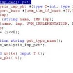
The old monitoring and logging approaches don’t work in the complex world of UVM. Those approaches are rather like trying to debug C++ at the C level. You need debugging methods that understand the complexities of classes, constrained random and other features. Synopsys has been working hard to bring interactive debugging up to the needs demanded by UVM testbenches, among other things a very cool ability allowing you to roll back time to discover the root cause of problems (a critical feature when dealing with randomized stimulus).
The Webinar is on July 20[SUP]th[/SUP] at 10am PDT. You can REGISTER HERE.
Web event: Time-travel in a SystemVerilog/UVM world – Interactive Testbench Debug Unleashed!
Date: July 20, 2016
Time:10:00 AM PDT
Duration: 60 minutes
The volume of testbench code and complexity of testbench environments have far surpassed those of the designs they verify. As teams migrate to SystemVerilog and UVM class-based testbenches for higher verification efficiency and increased verification reuse across projects, testbench debug remains the long pole. Traditional methods of debugging testbenches with waveforms and carefully crafted logging are unable to scale with modern testbenches. From testbench bring-up to constrained random simulations to regressions, inefficient testbench debug is what stands between verification engineers and their ultimate aim of finding a design bug.
In this Synopsys webinar, we will show how interactive debug is ushering in a new era in testbench debug. Specifically, you will learn:
[LIST=1]
Speakers:
Vaishnav Gorur
Product Marketing Manager, Verification Group
Vaishnav Gorur is currently Staff Product Marketing Manager for debug products in the Verification Group at Synopsys. He has more than a decade of experience in the semiconductor and EDA industry, with roles spanning IC Design, field applications, technical sales and marketing. Prior to joining Synopsys, Vaishnav worked at Silicon Graphics, MIPS Technologies and Real Intent. He has a Masters degree in Computer Engineering from University of Wisconsin, Madison and is currently pursuing an M.B.A. at University of California, Berkeley.
Mansour Amirfathi
Sr. CAE Manager, Verification Group
Mansour Amirfathi is currently Sr. CAE Manager for debug products in the Verification Group at Synopsys. He has more than 25 years of experience in the semiconductor and EDA industry, with roles in design and verification for wireless, graphic and signal processing. Prior to joining Synopsys, Mansour worked at Mentor Graphics as a High-level synthesis specialist. He has also held roles at Siemens, Cadence, Infineon Technologies and Cadis. He has a Masters degree in Communication from the University of Aachen in Germany (RWTH).