Introduction to IoT Analytics – IoT Analytics vs. BigData Analyticss. In the previous chapter of the IoT tutorial, we explained the affiliation between IoT data and BigData, given that IoT data expose the Vs of BigData. We also illustrated the activities comprising IoT data processing applications, such as data selection, validation, semantic unification and more.
Continue reading “IoT Tutorial: Chapter 8 – Introducing Internet-of-Things (BigData) Steams and Analytics”

IMEC-Horizontal Nanowires for 5nm at the VLSI Technology Symposium
At the VLSI Technology Symposium, IMEC presented a paper entitled “Gate-All-Around MOSFETs based on Vertically Stacked Horizontal Si Nanowires in a Replacement Metal Gate Process on Bulk Silicon Wafers”. I have wanted to blog about this paper since the symposium was held but also wanted to tie it in with an interview with someone from IMEC who worked on the technology. This last week I got a chance to speak with Dan Mocuta of IMEC about the work.
The first question you may ask is why Horizontal Nanowire (HNW) technology is interesting. In my previous blog on An Steegen’s “Secrets of Semiconductor Scaling” presentation I discussed the looming limits on FinFETs. Basically FinFET scaling is expected to end at the 7nm node (real node, 5nm node at the foundries). To continue to scale some type of new device structure is needed. HNW processing is very similar to a FinFET process and they provide improved electrostatics and scaling. Many researchers and leading technologists believe HNW will be the successor to FinFEts.
You can read my blog about An Steegen’s paper HERE.
In the IMEC work they created 2 – 8nm diameter horizontal silicon nanowires stacked on top of each other. The pitches are slightly relaxed from what is needed for a 7nm node in order to demonstrate the devices.
The process to fabricate the nanowires is as follows:
[LIST=1]
There are of course a number of adjustments needed to accommodate HNW fabrication versus FinFET fabrication but with the exception of steps 2 and 10 the process is essentialy the same as a FinFET process.
All of these details are available from the VLSI Technology paper. Looking at this flow I could see it was a single threshold voltage device and the lack of a raised SiGe source/drain for PMOS was a drawback. When I got to sit down with Dan Mocuda I asked him about the limitations in the work presented.
Dan said it is a 7nm process but somewhat relaxed to focus on the device behavior as opposed to pushing the process. The current work is also single Vt but they have been successful at CMOS integration with dual work functions. With respect to raised SiGe source/drains for PMOS there are integration challenges because of the SiGe etch to release the Si nanowires but they are working on integrating it using spacers to protect the raised SiGe source/drain.
The technology covered in this papers is also not a fully integrated process flow. For a full process you need ESD, I/O and multiple threshold voltages and they are working on all of that. I asked him if they might integrate FinFETs as part of the flow for I/O and he said there are ways to do that. You could selectively grow the Si/SiGe/Si/SiGe super lattice in one area and silicon in other areas to form FinFETs. This work was simplified version to demonstrate the technology and they are now working on smaller pitches and fully integrated process.
We also discussed the limits of FinFET technology. Ultimately gate pitch limitations in FinFETs drives the need for nanowires. Fin widths can’t be less than 5nm because mobility collapses and gate length can’t be less than approximately 18nm for electrostatic control. Nanowires have better electrostatic control than FinFETs and can provide additional gate scaling leaving more space for contacts. They also have simulation studies that show lower variability for HNW than FinFETs so low voltage performance is better.
One key area that still needs to be further evaluated for HNW is the vertical spacing between the wires. As the spacing between the wires gets smaller the process is simpler but if they get too close you lose electrostatic control.
In terms of timing Dan believes HNW will be needed in the early 2020s as a true 5nm technology and he thinks it can be ready. It is built on FinFET replacement metal gate technology and if you get on the development train now you can be ready in 3 to 4 years! Many of the leading technologists I talk to also believe HNW is the 5nm solution!
10nm Will Be an Epic Process Node!

In the history of the fabless semiconductor industry the foundries have always been a process node or two behind the leading semiconductor manufacturers. Starting in Q1 2017, for the first time in fabless semiconductor history, the foundries will have a process node advantage. This is horrible news for some but great news for others including myself.
You can ignore the “my process is better than yours” Power Point nonsense. Silicon does not lie and what silicon says is that you must be able to design to a foundry process and yield chips that will succeed at the system level, right? That brings us back to 10nm and the mighty fabless semiconductor ecosystem.
Clearly it takes an ecosystem to build a chip but it also takes an ecosystem with “relentless collaboration” to build a leading edge process that everyone can design to. A good example was illustrated at the Synopsys/Samsung “Ready to Design at 10nm” breakfast at #53DAC last month. Unfortunately I missed the free breakfast but the video is now up on the Synopsys website HERE and it is definitely worth your time. For full effect please load a plate up with your favorite breakfast food and grab a cup of coffee.
One of my favorite foundry speakers, Kelvin Low from Samsung Foundry, was on board. Let’s not forget, during Kelvin’s tenure Samsung was the first foundry to hit FinFET high volume manufacturing last year with their 14nm Exynos SoC and modem (Galaxy S6) followed by the Apple A9 SoC (iPhone 6s).
*SPOILER ALERT*
In case you are interested, Kelvin talks in detail about Samsung’s 10nm and 7nm foundry plans which are quite different from TSMC’s and GlobalFoundries’. Before Samsung, I knew Kelvin at GlobalFoundries and Chartered Semiconductor so I can tell you he is a very skilled foundry guy, absolutely.
The other guys on the panel were from Synopsys: JC Lin who spoke on Compiler II Technology Strengths for 10-nm FinFET and Andy Potemski who spoke on the 10LPE Reference Flow & ARM® Cortex®-A53 CPU Reference Implementation.
I do not know JC or Andy personally so I have included their biographies:
JC Lin
Vice President, IC Compiler II R&D, Synopsys
JC Lin has worked at Synopsys for more than 20 years. He has worked on multiple technologies and products, including logic synthesis, physical synthesis and place and route. His current focus is on the IC Compiler II place and route product. JC holds a Bachelor degree from National Taiwan University on Electrical Engineering and a Ph.D. degree from SUNY Stony Brook on Computer Science.
Andy Potemski
Senior Director, Foundry Reference Flows and Lynx Design System R&D, Synopsys Andy brings 36 years of industry experience to the table. He has been focused on design flows and automation since joining Synopsys over 21 years ago. Presently he is responsible for the Lynx Design System product R&D as well as foundry reference flow development. Prior to Synopsys, Andy spent 13 years as an IC development engineer with IBM. He holds 8 US patents in chip design and automation.
Can one process handle IIoT safety and security?
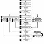
SemiWiki had another article recently making the case that in IoT applications, safety and security are intertwined, adding that both are important, but they are not the same thing. Mentor Graphics has weighed in with a new white paper trying to tie both issues to a methodology.
Industrial IoT – or IIoT as you’ll often see in shorthand – applications are rarely in a “greenfield”, meaning system designers can’t just do as they please. Instead, IIoT is most often operating in a “brownfield”, with legacy equipment and data and certifications that must be brought forward and integrated into the automation system.
As many have written including myself, security is all too often a major hole in IoT applications. Most firms have become hyperfocused on safety in automation, and the IIoT needs the same ‘-critical’ focus. The question for IIoT design teams is how to rationalize and incorporate both safety and security requirements. The brownfield may be a good thing, because designers are forced to deal with a range of issues.
Robert Bates, Chief Safety Officer at Mentor Graphics, sets the tone:
“Over the past decade, management of safety as part of system designs has gone from being something that we try to do the “best we can” to a much more formalized practice that can be used to greatly decrease the risk of economic damage, environmental harm, and risk to human life when things go wrong. This has been achieved through a systematic approach to safety management and incorporation of safety thought-processes in the product development process all the way from initial concept to end-of-life.”
Bates then submits that while some of the technology pieces differ, the thought process and methodology behind IIoT systems design for safety considerations can be reapplied to the security lifecycle. Where safety presents “hazards”, security presents “threats”, and interchanging those words in his list for an IEC 61508-compliant development process yields the following:
1) Define the concept and scope.
2) Perform a threat analysis.
3) Classify the threats by levels [to some specification].
4) Define security requirements for each device to mitigate the identified threats.
5) Plan for realization of the device.
6) Develop the devices components in terms of both hardware and software.
7) Integrate the device components.
8) Validate that all security requirements are fulfilled.
It’s an interesting idea that an IEC 61508 framework could apply, but those familiar with security practices will immediately see a couple of points that need further exploration. First, we don’t have a good list of industry-recognized threat levels that would help with selection or evaluation of hardware and software for compliance – something the folks at NXP have postulated recently, and I’m sure others are thinking about this. (“Does this microcontroller meet the parametric requirements for Security Level X?” The levels, and the parameters, are open for discussion. Common Criteria levels are a starting point but don’t cover some embedded needs.)
Second, there is the idea that absolutely nothing is absolutely secure. Threats are a moving target; one is limited by what good system design, penetration testing, and shared threat information know at a particular point in time. The problem for IIoT design is experience with many current threats simply does not exist in organizations who haven’t had industrial devices broadly connected to enterprise networks. Blending IT and OT skills is a must in designing a system that is as secure as possible when deployed, and can evolve rapidly to respond to new threats.
After describing the above list in an IEC 61508 safety context, Bates makes the leap:
“The main takeaway here is that once a solid safety process is in place, expanding that process to ensure security is straightforward. The main differences are at the beginning, where identifying the security threats is a practice that will be unfamiliar to system engineers who already understand identifying safety hazards, and at the end where different verification techniques such as penetration testing might be required. This gap can be closed with training, or by bringing on additional expertise (like hiring a security manager who works hand-in-hand with your safety manager).”
The entire Mentor Graphics white paper is available for download via registration:
Building Functional Safety and Security into Modern IIoT Enterprises and Ecosystems
This is the right kind of discussion. The IIoT definitely needs some type of structured approach if devices are to have any hope of broad interoperability, including security aspects where the weakest link principle applies. Since many IIoT teams are already working in an IEC 61508 framework, extending that approach to address security may help close the gap.
Samsung Embraces Both Public And Private Cloud With Joyent Acquisition
As the mobile industry growth slows and looks to growth in IoT, companies like Samsung Electronics are looking for ways to initiate change or adapt to the new climate around them. One of the ways mobile companies are going to be profitable in the future is through offering, building and sometimes hosting those services beyond just selling the device to the consumer. Some mobile companies have already done this like Apple (iCloud), Google (Google For Work), Microsoft (Office 365) and in PCs, HP (TouchPoint Manager) and Dell (ProSupport Plus). Offering services after or part of the sale is a way for mobile smartphone manufacturers to be able to continue to earn incremental revenue and profit after they’ve already sold the phone and provide more of a holistic solution. Samsung’s acquisition of Joyent aligns with those trends and the company’s long-term objectives.
No mobility without the cloud
Mobility wouldn’t exist as we know it today without the cloud. You see, behind every fancy mobile app and service is a giant datacenter that hosts the “back end” of the app, or where the heavy lifting happens. This is why the largest capital expenses for Google, Microsoft, Facebook and Amazon are datacenters and the biggest trend in the enterprise iOS the race to the private cloud. At Moor Insights & Strategy, we cover this trend every day, whether the “Super 7″ public cloud giants or the up and coming private and hybrid cloud players like Dell and Hewlett Packard Enterprise.
Samsung already does cloud, but expensively
Samsung has been heavily relying on Amazon.com AWS and Google for their cloud services which many Android OEMs have done in the past. However, with the need to drive profitability and service “stickiness” on a global scale, paring back their external cloud spending could be a potential opportunity for Samsung to both offer new enterprise and consumer services while also reducing their external cloud expenditures.
What Samsung could do with Joyent
Samsung isn’t detailing exactly what it will do with Joyent right now for obvious, competitive reasons, but I will talk about what they could do with it. Joyent brings a lot of things to Samsung that could make sense for the company’s consumer and enterprise businesses including their own cloud infrastructure, end to end container solution as well as many other cloud services. Joyent was one of the few companies left in the cloud space that hadn’t been acquired by a big company like Samsung.
Samsung already has a plethora of different services that they have to support across a broad array of products that the company sells. While this acquisition has been made by Samsung’s mobile division and will allow Joyent to operate as a wholly owned subsidiary, there are still many opportunities for other Samsung divisions to utilize Joyent’s infrastructure.
IoT leadership requires cloud competency
Samsung Electronics, like its competitors, is moving heavily towards IoT and enabling consumer IoT solutions through their acquisitions like SmartThings and there is only going to be an increased demand for cloud services to service those IoT devices. Since IoT includes Smart TVs, that also means that Samsung could potentially host much of their own content delivery platforms and run many of their future planned services on their own infrastructure instead of Amazon or anyone else. Acquiring Joyent would also allow Samsung to be able to increase the size of their Samsung Pay service to more geographies and scale the service globally without incurring too many external cloud costs.
The acquisition of Joyent also means that Samsung could more efficiently offer custom tailored private cloud solutions to their enterprise customers that are utilizing Samsung’s devices for business uses. Samsung has their own Knox enterprise platform which can now operate wholly off Joyent’s infrastructure and enable a secure end to end solution for Samsung’s customers, something that many enterprises are looking for these days. Additionally, it allows Samsung to improve their enterprise offerings to match those of their mobile competitors and not to rely on the offerings of companies like Amazon.com AWS, Google and Microsoft Azure to sell services to customers. The recurring revenue that can be generated from these services is what companies like Samsung Electronics desperately need in a smartphone market that is huge but without growth.
Wrapping up
Samsung’s move to acquire Joyent makes sense on the surface for a lot of reasons. Both companies have a lot of benefit from one another, and Samsung is smart to not wholly absorb the company into the Samsung corporate structure and allow it to operate independently. By giving Joyent a bunch of its own business and improving Joyent’s scale, they could also improve Joyent’s market share as well as profitability. Samsung also gives Joyent a great platform to test many of their new services on and to give Samsung the first opportunity to utilize those services and to differentiate Samsung from their competition. Joyent’s infrastructure should be helpful in enabling Samsung’s data-rich future and increased demand for cloud services through new product offerings and associated cloud services, not to mention getting reducing costs by stepping away from Amazon.com AWS.
Big Data Lessons from the LHC
Big Data techniques have become important in many domains, not just to drive marketing strategies but also for semiconductor design, as evidenced by Ansys’ recent announcements around their use of Big Data analytics. And they should become even more important in the brave new world of the IoT. So it makes sense to look at an organization that is managing bigger data than anyone else in order to understand approaches we may need as we scale.
Before we think about measurement data, CERN (the organization that host the LHC) uses Big Data analytics for control, for the accelerator and instrumentation, independent of data gathering. Why? Because running an accelerator of this class is very complicated. You are accelerating charged particles at very close to the speed of light around a very-high-vacuum tube 27km in circumference, which takes many vacuum pumps, many cryogenic systems, many power controls, many sensors. And that’s just the main accelerator. Add to that the ion source that feeds the accelerator, control for multiple complex detectors and you have a system more complex than any other I can imagine.
Managing all of that is first a giant sensor / actuator / feedback problem (like using IoTs for maintenance on a massive scale) and second a big data problem because the data gathered from those systems is necessarily massive (in one example, just the cryo data runs to a billion records). Complexity is high enough that the system as a whole is in a fault-state 37% of available time. CERN decided that preventive maintenance is not enough to get maximum value out of the LHC, and since they want to plan for the next generation which will be even bigger and more complex, they have worked with multiple partners to build a Big Data analytics systems to better forecast potential problems before they happen.
This is where IoT for maintenance is already moving – not just knowing when something is broken, or scheduled for repair, but being able to do predictive analytics. Perhaps there will be synergies between the work being done at CERN and in other enterprises. Hopefully Oracle (who play a big role in the CERN control systems) can exploit some of these synergies.
The control aspect is critically important, but when most of us are thinking about Big Data and the LHC, we’re probably thinking about managing measurement data – the information that leads to new physics. The largest detector (Atlas, pictured above) generates ~1 petabyte per second of data, far beyond levels you could consider storing. And the vast majority of the data is uninteresting anyway because it only contains known collision events and the goal is to find new physics.
Filtering has to reduce a O(10[SUP]9[/SUP]) event rate to O(10[SUP]2[/SUP]) with low probability of rejecting interesting events, which they accomplish using a series of specialized and massively pipelined triggers (traditional compute would be far too slow for the first stage of triggers). Only after this filtering is data then set on for further processing and storage. The parallel for the IoT world is that no, you can’t just ship all data to the cloud. You have to pre-filter and, depending on how much data your devices produce, you may have to pre-filter very aggressively using very sophisticated logic.
The data that survives filtering still amount to ~30PB/year. This data falls in the Big Data class of “never throw it away”, since you don’t know in advance how it may be used in different analyses. So you want permanent storage, but what you may find interesting is that this is not on disk – it goes to a tape archive (who knew we still had tape?). In fact, they have ~100k processors writing at peaks of 20GB/s to 80 tape drives. The rationale for tape is that cost is still a lot lower than for disk and power requirements are zero when a tape is not being accessed. And since generally users of the data don’t require instantaneous access across the whole dataset, performance is not an issue.
On the other hand, you lose a lot in random access flexibility with tape, so a catalog of metadata is stored online. Once you’ve found what you need, a tape robot will load the appropriate tapes. Could we ever see this for IoT cloud data (or the cloud in general)? There’s arguably a security issue in tapes you can carry away, but since the whole thing is managed by a robot, you might actually have better physical security around a tape vault than we see in conventional systems. Then again maybe we’ll eventually see higher density read-only material advances (an upcoming blog) that will replace both disk and tape.
CERN Big Data is definitely far bigger and far more challenging than we are likely to see in the IoT for some time. Still, I find it interesting to look at how they handle data to get some idea of where we may eventually find ourselves. You can learn more about Big Data for control at the LHC HERE and Big Data for measurement HERE. For the truly dedicated, you can learn about how CERN does real-time filtering of measurement data HERE.
Not-so-ulterior motive leads SoftBank to ARM
This week’s £24.3B offer for ARM Holdings plc from SoftBank has been widely viewed as Brexit reflexit. It did firm up in the preceding two weeks, but this acquisition offer has been years in the making – and if it sticks, one SoftBank motive many analysts and editors are missing comes front and center. Continue reading “Not-so-ulterior motive leads SoftBank to ARM”
Electrical-Optical Design, A Bridge to Terabitsia

If you don’t get the tongue in cheek reference of the title, you probably don’t have children who liked to watch Disney movies. All four of my daughters loved Disney and so, I am forever shaped by the Wonderful World of Disney. In 2007 Disney adapted to the screen a novel called, ‘A Bridge to Terabithia’, in which two adolescents escape (at least temporarily) into a make believe world of wonder and magic. Sometimes when I read about all of the work going on in electrical-optical (E-O) design I get the feeling I’ve been dropped into such a magical world.
In one of my previous articles, “TheGuiding Light and Other Photonic Soaps”, I brought out the dichotomies between electronic and photonic design and exhorted all to us to think hard about the need for building bridges between electronic and photonic design automation tools, later referenced as EPDA tools. It seems that some of these bridges have already been built and that there has been much progress towards putting together viable E-O design flows. Friends in the EPDA world provided me with existential proof of the work that is pulling these two very diverse industries together. Examples cited included a host of papers about silicon photonic design rule checking, equation based DRC verification methodologies, scalable photonic design environments using PDKs, LVS checking for photonic ICsand even two books that talk extensively about design flows for E-O type designs (Silicon Photonics IIIand Silicon Photonics Design: From Devices to Silicon).
They also pointed to E-O bridges that have been built between Mentor’s Pyxiscustom design tools and Calibre ICverification tools with photonic tools from Lumerical Solutionsand PhoeniX Software. In this cited flow Mentor’s tools are responsible for the electronics portion of the design while Lumerical’s circuit simulator, INTERCONNECT, is used to simulate the optical portions of the design and PhoeniX Software’s OptoDesignersoftware is used to do photonic waveguide routing. All of these tools are working in a fairly integrated environment allowing designers to share information back and forth between the electrical and optical domains. A similar flow has also been put together between Mentor’s Tannercustom design tools and Luceda Photonics’ IPKISStool. I’m told that all of these tools have been deployed at several customer sites and are now being put to the test on real E-O designs looking to operate in the Terabyte-per-second regime. Thus the tongue-in-cheek reference to Terabitsia, except in this case it’s not magic. It’s real!
On a related but different front, there are also a growing number of photonic training sessions being given around the world to bring more electronic and photonic designers up to speed on these new E-O flows. Examples of this include an edX course entitled, ‘Silicon Photonic Design, Fabrication and Data Analysis’ hosted by Professor Lukas Chrostowski of the University of British Columbia. In Professor Chrostowski’s course students used a cloud-based training environment that used the Mentor Pyxis and Lumerical INTERCONNECT tools to learn how to design, fabricate and test photonic circuits. Student designs were fabricated and tested and results were sent back to the students for them to analyze how their design really worked after manufacturing. In his next edX course, Professor Chrostowski will be showing new methodology developments and his approach to simulating on-chip device and waveguide variation. This is becoming more important as photonic IC designs scale in complexity.
Similarly, an industry group known as plat4Mis collaborating with the Europe Silicon Photonics Alliance (ePIXfab) and several EPDA vendors to host a Silicon Photonics Summer School in August of this year at Ghent University, in Belgium. This hands on session will use the Mentor Tanner and Luceda tools to train participants in silicon photonic design, circuit level simulations and design-rule compliant layout using PDK-based design methodologies.
Lastly, no bridge is useful without a firm foundation and in this case that foundation comes in the form of electronic and photonic process design kits (PDKs). Plat4M, a European funded project to enable a seamless transition of silicon photonics research platforms to industry and ePIXfab, an open alliance of European organizations who mission is to promote silicon photonics science and application, have been instrumental in working with EPDA vendors such as Mentor Graphics, PhoeniX Software and Luceda towards the offering of well-characterized photonic PDKs that can be used in these new E-O based design flows. This has been echoed by PDK offerings from a multitude of photonic foundries such as imec,CEA-Leti,ihp,VTT,SmartPhotonics,Fraunhofer HHI,LioniX,Oclaro,IMEand now Sandia National Labsand theAIM Photonicsinitiative in the United States.
While E-O designs are not wide-spread yet, interest in their application is growing and becoming more important in areas such as Telecom, Datacom, Space and Defense, Sensors, Security, Transport, Energy and Environment to name just a few. Perhaps the bridges being built are indeed leading us to Terabyte-per-second speeds and a whole new world that will indeed seem like magic!
Technology, Shakespeare, Linguistics and Combatting Terror
My brother Sean is working on post-doctoral research in linguistics, especially the use of language in Shakespeare’s plays. Which may seem like a domain far removed from the interests of the technologists who read these blogs, but stick with me. This connects in unexpected ways to analytics of interest to us techies, and ultimately to a topic of interest to every reasonable person worldwide.
Let me start with Sean’s research. His goal has been to understand the different use of language, for example pronouns, between soliloquies in the comedies, history plays and tragedies. I won’t tax the patience of SemiWiki readers by going into the details – if you want to know more, there’s a link at the end of this blog. His approach is based on something called Corpus Linguistics – analysis of a body of writing to find trends and correlations.
Since Shakespeare’s works, prolific though he was, fit comfortably into one large, small-print volume, analysis of an electronic version can be performed easily with desktop software. Think of a statistical analysis package applied to language rather than numbers, looking at frequencies of word usage, or words used in close proximity. There are multiple software packages (from small and probably mostly academic vendors) for this type of analysis.
Automated analysis of language depends on recognition, and recognition at a basic word level can be very straightforward; even recognizing inflected words as variants of the base word is not complex in English. Going further than word recognition requires tagging the text (“this is the subject in this sentence” for example) or some level of natural language recognition, which gets you into the domain of Google’s SyntaxNet and deep-learning technologies.
Corpus Linguistics methods are not limited to published works. Domains within the Internet are obvious candidates for analysis, where Big Data analytics and deep learning methods can be valuable. But to what purpose? There are perhaps lots of interesting market analyses that could be done in this way, but one much more compelling application is to detect impending terrorist attacks.
Sean’s own department (at Lancaster University in the UK) is active in research in this area, as are a number of other universities. Each group is predominantly looking at social media posts from identified terrorists. The Lancaster group are looking at word “collocation”, measuring the closeness of connection between significant words and the name of a person or place. “Attack” and “crowded” would be an obvious example. This can be used to establish positive or negative associations; increasing frequency of such connections then potentially indicates an upcoming attack.
While approaches like this are clearly not foolproof, they can provide valuable supporting evidence when combined with other indicators. Also for me this general domain illustrates opportunities we often miss in sticking to our own silos of expertise. Technologies that we do understand are often used in domains far from those we might expect. And bigger pictures, combining needs and techniques from widely differing domains, can often suggest solutions that silo experts might miss.
You can learn more about Sean’s research HERE and the work on terrorist post analysis HERE.
10 Challenges in IP Design Collaboration

Enterprise design management can be summed up in one word: collaboration. Intellectual property (IP) reuse and the success of distributed system-on-chip (SoC) design efforts depend strongly on how well designers can collaborate. As time-to-market windows have shortened, the challenges around design collaboration have become more critical.
With escalating design costs for each SoC start, shouldn’t there be more emphasis on an underlying design management engine to maximize designer productivity and team efficiency? During my visit to #53DAC, I saw a sneak preview of just such a new collaboration platform in development at ClioSoft – and we shared our views on this Top 10 list of challenges ClioSoft is targeting.
Trivial designs and very small teams aside, most IP/SoC design efforts run into many, or all, of these challenges. Improving IP/SoC design collaboration has many of the same characteristics as any major change initiative, and has some IP-specific issues.
10) Multi-site teams can’t keep data in sync real time: With large teams collaborating across multiple remote sites, often worldwide, keeping the design data in sync securely and in real time is key to improving design productivity. Some remote sites do not have the requisite network bandwidth available, making it more important to ensure optimal use of bandwidth.
9) Revision control and release management must be managed: With different teams working on the same design, it becomes important to manage the different design versions as well as to identify the differences between the versions for both text and binary files. Integration with EDA tools to check in or check out different versions of a design is a definite plus.
8) Information is trapped in silos: As with many business processes, organizational structure is sometimes a barrier to sharing. It’s not even the overt “warring tribes” mentality; it can be as simple as business units not regularly interfacing with each other in open conversation. Any knowledge or IP developed within a business unit does not necessarily get shared with other design groups.
7) Physical boundaries are in the way: Distance, time, and language are the traditional barriers to collaboration. Time zones, different work tools, different expertise domains (digital versus analog, timing versus power, IP block versus system integration, and so on), different patterns of responsiveness, and different preferred mediums of exchange can also be barriers.
6) Multiple unconnected sources of information can lead to mistakes: Design information is typically captured in different tools and formats; for example, in meeting notes, emails, Word documents, Excel spreadsheets, bug tracking systems, or design management systems. To avoid costly mistakes, everything relating to a project should be stored in one place for all to see and use the correct versions.
5) No clear guidelines on what should be shared: Most designers are still not sure what data can be shared with others within a company or with vendors or externally. Who has access to what design data should be determined by built-in and customizable access restrictions and by ensuring that all design data is stored in one place.
4) Unclear information on third-party IP: In-house built IP, borrowed IP, and bought IP may have three different sets of artifacts and metadata. Bought IP may be the hardest one to obtain data for. Vendors may be unwilling to share, or may charge for the privilege, or may just not have some elements of data. In addition, while accessing third-party IPs, most designers do not pay attention to the license agreements to see if they are authorized to use the IP, which can lead to liability problems.
3) Limited feedback between IP authors and users: IP artifacts tend to flow downhill, from creation of individual blocks to integration of subsystems and finally the full-up SoC. Creators often do not find out what happened from users of their IP, but that information can be critical to future reuse. IP users, on the other hand, do not know how to fix IP-related problems and often end up creating a kluge to resolve issues. If users know the IP authors, they can communicate with them for any needs.
2) Tracking IP quality is difficult: What should be tracked regarding IP quality? A database is only as good as the items captured; reporting depends on metadata describing variables and relationships. Thinking through quality metrics can help decide what to track.
1) No infrastructure for sharing and reusing IP: Replacing “sneakernet” with an “intranet” moves documents, but not real information. Design data and IP need an enterprise tool designed for collaboration optimized on an infrastructure that delivers cost-effective performance.
Do the items on this list sound familiar? What else is holding back more IP reuse, or driving up SoC design costs in terms of productivity, in your organization?
Also Read
Enterprise design management engineered for SoCs