This interview originally appeared as the foreword to our book “Prototypical: The Emergence of FPGA-based Prototyping for SoC Design” but I thought it would be worth publishing for those of you who have not downloaded it yet. I also wanted to mention that our friends at S2C are currently offering a 50% discount on the Prodigy Kintex UltraScale Prototyping Solution Package to get you started on your prototyping journey.
Remember, the health of the semiconductor industry revolves around design starts which translate to wafer starts and ultimately product shipments. If all goes well the semiconductor industry continues to grow and we live happily ever after, right?
Unfortunately, all does not always go well with design starts and nobody knows that better than Mon-Ren Chene, the CTO of S2C. His 30+ year semiconductor career spans: EDA, FPGA, Emulation, and FPGA prototyping so he is definitely the right person to ask about a successful design start:
Nearly two decades ago during our time at Aptix, my S2C co-founder, Toshio Nakama and I recognized the power of prototyping. At that time, prototyping was only accessible by large design houses with the budget and means to employ a prototyping architecture. We also recognized that FPGAs had become a popular alternative to the much more expensive and rigid ASICs. It was then that we both decided to team up to develop a prototyping board around an FPGA, and S2C was born. Our commitment to our customers has been to push the limits of what FPGA prototyping can do to make designing easy, faster, and more efficient.
Our goal has always been to close the gap between design and verification which meant that we needed to provide a complete prototyping platform to include not only the prototyping hardware but also the sophisticated software technology to deal with all aspects of FPGA prototyping. Fast forward to today and you’ll find that FPGAs and FPGA prototyping technology has advanced so much that designers and verification engineers can no longer ignore the value that they bring, especially when dealing with the very large and complex designs that we see today. These advances have made FPGA prototyping poised to become a dominant part of the design and verification flow.
This book will hopefully give you a sense of how this is achieved.But what’s next for FPGA prototyping? Having dedicated my time to working with our customers in developing the evolution of FPGA prototyping, I have figured out two things: FPGA prototyping needs to be part of the conversation early on in the design process, and FPGA prototyping needs to move to the cloud. What do I mean by these two statements? Well, let’s break it down.
Design for FPGA Prototyping
Making FPGA prototyping part of the design process early means actually thinking about how the design will be prototyped via an FPGA as you design – Design for FPGA Prototyping. Designing for prototyping will significantly speed up the FPGA prototyping process downstream. It will aid in the act of synthesis, partitioning, and debug. I’ve outlined six ways that this is achieved:
(1) Prototyping-friendly Design Hierarchies Design architects can make the job of prototyping much easier for engineers to implement FPGA prototyping by modifying the design hierarchy to work better in a prototyping environment. The engineers who perform implementation or verification usually have very little ability to improve prototyping performance once the design hierarchy is fixed. The need to do partitioning down to the gate level can be removed if the size of each design block can be kept to one FPGA. Furthermore, modifying the design hierarchies early can help to avoid pin congestion as many times a design becomes very difficult to implement in an FPGA or becomes very slow because there’s a central block that has tens of thousands of signals that need to go to multiple blocks in different FPGAs. Design architects can also ease prototyping by providing guidance to their FPGA implementation team(s).
(2) Block-based Prototyping
Instead of hoping the entire design will magically work when mapped and downloaded to multiple FPGAs, bringing up subsystems of the entire design, block by block, will allow quick identification of both design issues in a sub-block as well as any issues related with mapping the design to the FPGA(s). Blockbased prototyping works well especially with designs that contain many 3rd party IPs that also needs a lot of real time testing and early software development.
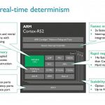
And very often, designers don’t even have the RTL source code for the IP blocks from 3rd parties (for example, ARM processors) and therefore cannot map the IP to the FPGAs themselves. This can be solved by requesting the IP provider to supply the encrypted netlist so that you can synthesize and partition the entire design while treating that IP as a black-box. As long as you specify the correct resources (LUT, registers, I/Os), the prototype compile software should take those resources into account when partitioning to multiple FPGAs. You can then integrate the encrypted netlist during the place and route stage.
I’ve come across customers that want to do an FPGA implementation but are reusing some very old blocks with only the ASIC netlist and without RTL. Implementation becomes very difficult since the details of the design are unknown. These legacy designs are usually only accompanied by a testbench. In this case, the best approach is to covert the ASIC gates to an FPGA and to use a co-simulation environment (such as S2C’s ProtoBridge™) to verify if the functionality of the block is correct before integrating it with the entire design. Unfortunately, this is still a painful process so designers should consider either not using those legacy blocks or re-writing them.
Note that a reconfigurable and scalable prototyping system is needed for a block-based prototyping methodology, as well as a robust partitioning and FPGA prototyping software flow.
(3) Clean and Well-defined Clock Network for Prototyping
Many ASIC designs have tens or even hundreds of clocks and most of them are just for power management/saving. Even with the most complex designs there are usually a few real system clocks plus some peripheral clocks such as PCIe and DDR. Peripheral clocks usually reside in a single FPGA which has the actual external interface pins and therefore are easy to implement. System clocks, however, need to go to every FPGA and therefore should be clean for FPGA implementation.
ASICs use a lot of gated clocks to save power. Today’s FPGA synthesis tools have advanced to take care of most of the gated clocks, but there may still be some gated clocks that go undetected and therefore cause design issues. This can easily be avoided by creating two different RTL clock implementations for the ASIC and the FPGA by using IFDEF.
Internally generated clocks can also be a problem for an FPGA prototyping environment as they all need to get on the FPGAs’ global clock lines and synchronize among all the FPGAs. A Multi-FPGA prototyping system will have a limitation on how many of these global clocks can be supported therefore the number of the internally generated clocks should be restricted (or again use two implementations in the RTL: one for ASIC, and one for FPGA).
4) Memory Modeling
ASICs support many different types of memories while FPGAs usually support two types: synchronous dual port memories, or the use of registers and LUTs to build custom memories. The latter one consumes large amounts of logic resources and might cause place and route congestion. Most ASIC memories can be re-modeled to take advantage of the block memories in the FPGA but a manual process may be required to do that. Again, instead of having the engineers who try to implement the ASIC design in a FPGA model the memories, a better approach would be to have the architects plan the designs with two memory implementations both for ASICs and FPGAs. The RTL designers then code using IFDEF to have the two implementations. FPGA prototyping becomes easy by just instantiating the correct memory implementations.
5) Register Placement on the Design Block I/Os
FPGAs usually have a lot of register resources available for the design but most ASIC designs try to use less registers to save area and power. Ideally, all block I/Os should be registered for FPGA implementation to achieve the best results. At a minimal all outputs should be registered so no feed-through nets (which impact system performance by half) will be created after design partitioning. As a result, there will be a noticeably higher FPGA prototyping performance with this approach.
6) Avoid Asynchronous or Latch-based Circuits
Asynchronous circuits and latch-based designs are FPGA unfriendly. It is very hard to fine-tune timing in an FPGA with every FPGA having to be re-place and re-routed multiple times. These issues become even worse when the asynchronous circuits have to travel across multiple FPGAs.
Moving to the Cloud
We are living in an age where design teams no longer reside in one geographic location. No matter how big or small, companies have multiple design teams in multiple locations. A cloud-based FPGA prototyping system is an ideal way for dispersed teams to manage the prototyping process and resources.
Furthermore, as smaller IoT designs proliferate the market, FPGA prototyping must become accessible to these designers. Today’s FPGA prototyping, although effective, can be costly for smaller IoT designers to adopt. The reusability of boards becomes less viable so costs cannot amortized over multiple design starts. By moving to the cloud, FPGA prototyping solutions can become a shared resource and thus can
reduce cost inefficiencies. The future of FPGA prototyping is strong. It has and will continue to demonstrate itself as one of the most effective solutions to realizing the full potential of any design.