RVN! 26 Banner revised (800 x 100 px) (600 x 100 px)

Advanced ASICs – It Takes an Ecosystem

Advanced ASICs – It Takes an Ecosystem
by Mike Gianfagna on 11-26-2017 at 2:00 pm

I remember the days of the IDM (integrated device manufacturer). For me, it was RCA, where I worked for 15 years as the company changed from RCA to GE and then ultimately to Harris Semiconductor. It’s a bit of a cliché, but life was simpler then, from a customer point of view at least. RCA did it all. We designed all the IP, did the physical design, owned fabs, assembly and test facilities and took full responsibility for every custom chip we built from handoff to volume production. We even developed and supported a complete suite of design tools. It was called CAD then, not EDA.

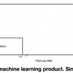
Things are different now. Building a custom chip now requires a lot of contributions from a lot of companies. Design, fab, packaging, IP, test and EDA are all delivered by different organizations with a laser focus on doing a particular part of the job very well. If you look at the challenges of FinFET and 2.5 designs for markets such as the cloud and AI, the complexity and number of players goes up yet again due to things like HBM memory stacks, interposers, advanced packages and enabling IP.

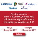
It is against this backdrop that I am pleased to say, “help is on the way”. eSilicon has been working with an extended family of ecosystem partners for many years, and a group of us will be taking it on the road soon, in Shanghai and Tokyo, to show how a team of companies can work as one to deliver advanced ASICs. We’ll be presenting at the Tokyo Conference Center, Shinagawa, Japan on Monday, December 11 and at the Kerry Hotel, Pudong, Shanghai, China on Thursday, December 14.

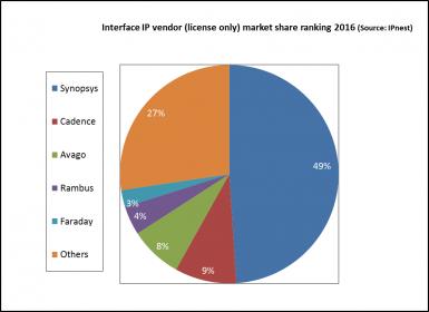
Over the course of the day from 10:30 AM to 4:00PM, you’ll hear from Samsung Memory about their HBM2 solutions, Samsung Foundry about their advanced 14nm FinFET solutions, ASE Group about their advanced packaging solutions, eSilicon, about their ASIC and 2.5D design/implementation and IP solutions, Rambus about their high-performance SerDes solutions and Northwest Logic about their HBM2 controller solutions. A complete ecosystem to address the requirements of advanced ASICs for markets such as high-performance computing, networking, deep learning and 5G.

There will also be cocktails and networking from 3:00PM to 4:00PM, with many very interesting lucky draw prizes to award.

Find out more about this valuable event and sign up to attend. It’s free, but space is going fast. We hope to see you there.

AbouteSilicon

eSilicon is an independent provider of complex FinFET-class ASIC design, custom IP and advanced 2.5D packaging solutions. Our ASIC+IP synergies include complete, silicon-proven 2.5D/HBM2 and TCAM platforms for FinFET technology at 14/16nm. Supported by patented knowledge base and optimization technology, eSilicon delivers a transparent, collaborative, flexible customer experience to serve the high-bandwidth networking, high-performance computing, artificial intelligence (AI) and 5G infrastructure markets.

Related Blog


Worldwide Interface IP Revenue Grew by 13.5% in 2016 (Source: IPnest)

Worldwide Interface IP Revenue Grew by 13.5% in 2016 (Source: IPnest)
by Eric Esteve on 11-26-2017 at 2:59 am

IPnest has released the 9[SUP]th[/SUP] version of the Interface IP Survey, ranking by protocol the IP vendors addressing the Interface segments: USB, PCI Express, (LP)DDRn, MIPI, Ethernet & SerDes, HDMI/DP and SATA. When the 1[SUP]st[/SUP] version has been issued in 2009, the IP segment was weighting $225 million and the 2009 to 2008 growth was negative due to the 2008 economic crisis. The same segment has generated $550 million in 2016!

As you can see on the below chart, Synopsys is clearly leading with 49% market share, followed by Cadence and Avago, each company enjoying about 10% market share, Rambus and Faraday ending this top 5 with less than 5% market share. In fact, as the interface IP market is essentially made of up-front license, IPnest has not included royalty in this ranking. If we take royalty into account, Rambus share would grow up to the Cadence level.

Since the first research, IPnest has built this survey by protocol, offering vendor ranking and competitive analysis for all the above-mentioned protocols. That’s why it’s possible to more precisely monitor the evolution of this dynamic market by protocol and for example compute the CAGR for each of the top 5 protocols: USB, PCIe, (LP)DDRn, MIPI and Ethernet & Very High Speed (VHS) SerDes. This ranking by CAGR appears on the below chart. If you compare USB and MIPI, what you see is that USB IP segment is much larger than MIPI (the smallest of the top 5), but that MIPI IP 25% CAGR is the largest, when USB IP segment has the lowest CAGR with 9%. But USB is, with Ethernet, the oldest protocol, issued in the 1990’s, when MIPI is more recent (mid 2000’s).

In fact, you can find much more information in this report, like the evolution of the number of design starts by protocol, as well as the evaluation of the number of commercial design starts, when a SoC integrates a specific interface IP externally sourced. This methodology allows to build 5 years forecast, that IPnest do every year. Obviously, you need a bit more than Excel to build such a forecast, let’s call it “IP intelligence”. You need to know the market trends for each protocol, the expected pervasion of specific protocol in market segment where it wasn’t used before (like PCI Express in automotive) … that’s why I spend so much time at phone or reading IP related news! But the result is satisfying, and no customer has ever complained about IPnest forecast accuracy, usually in the 5% to 10% range at 5 years at worst. Which is useful when you do the same work for about 10 years is that you can verify at year Y+5 the validity of the forecast made 5 years ago, at year Y…


For example, I can predict today that the Interface IP market will pass the $1 billion mark in 2022, growing at 12% CAGR between 2016 and 2022


This lead to another interesting point: the relative weight of the Interface IP segment in respect with the total Design IP market. As shown in the “Design IP Report” issued in 2017 by IPnest, the total IP market was $3.423 billion in 2016 and the license part was $1.956 billion. If we compare the license only revenue generated by the interface IP ($530 million) with the total license revenue, the interface IP segment is weighting 27% of the total.

In other words, the (license part) revenues of the interface IP segment is equivalent to the (license part) revenues of the processor IP segment (CPU, GPU and DSP).

But the main difference is that the processor IP segment is generating royalties, and the royalty share of the design IP segment has reached almost $1.5 billion in 2016, or 19% YoY growth!

If you work in a company addressing design IP, you should feel safe about future as this market has grown by 13% last year (9% for license revenues, 19% for royalty revenues). If your company address interface IP, you must know that this segment has grown by 13.5% in 2016 (licenses only), and will grow with 12% CAGR up to 2021.

IPnest has noticed some very interesting points: if Synopsys is the clear leader with 50% market share, this segment is becoming attractive, and different players attack this market. Rambus is well-known for patent licensing, but the company is now repositioning on IP licensing, the Snowbush IP group acquisition is a strong signal sent to the market.

Another group of vendors, the ASIC companies, is becoming very active in the interface IP segment. We can mention Invecas, working closely with GlobalFoundries, who is building a strong interface IP port-folio by acquisitions (Kool Chip, Krivi and Lattice IP group).

Nevertheless, the strongest Synopsys competitor is must probably Broadcom Ltd. (LSI Logic + Avago + Broadcom), even if the company doesn’t position as an IP vendor as they only sell IP like VHS SerDes to their ASIC customers.

If you consider the size of the interface IP market, reaching $950 million in 2021, there should be room for multiple players… but the winners will be the vendors building a strong engineering team, able to manage advanced PHY solutions based on VHS SerDes and supporting PCI Express and Ethernet running at 32 Gbps (PCIe 5.0) and 112 Gbps (PAM 4 SerDes for 100G Ethernet). And also able to address mainstream customers, offering one-stop-shop solutions targeting wide technology node spectrum…

Eric Esteve from IPnest

Just contact me at eric.esteve@ip-nest.com if you need more information about:
– the “Interface IP Survey 2012-2016 – Forecast 2017-2021”
– or the “Design IP Report” 2017


Seeking Solution for Saving Schematics?

Seeking Solution for Saving Schematics?
by Tom Simon on 11-24-2017 at 7:00 am

Schematics are still the lynchpin of analog design. In the time that HDL’s have revolutionized digital design, schematics have remained drawn and used much as they have been for decades. While the abstraction of HDL based designs has made process and foundry porting relatively straightforward, porting schematic based designs largely has remained difficult and time consuming. Fortunately, Munich based MunEDA has just significantly upgraded their schematic porting tool called SPT. Even more fortunately I had the opportunity to travel to Munich to attend the MunEDA user group meeting in November to learn more about SPT and their other offerings. While I missed Octoberfest, the MunEDA team made the event extremely worthwhile and even entertaining.

Rather than starting from scratch, reusing an existing schematic can save a lot of time, and preserves the initial investment in its development. For this to happen several distinct steps are needed. The devices in the existing design need to be converted to the corresponding devices in the new pdk. Rough scaling should be applied to arrive at preliminary property values. The placement, scaling and orientation of the symbols must be adjusted to match the original. Terminals that have name changes must be dealt with. Lastly any new or deleted terminals have to be accounted for.

Without a porting tool there are only a few alternative methods to accomplish the porting task. In Virtuoso ad-hoc or custom Skill code could be written, but this replaces a schematic editing task with a coding task – one that is not necessarily any easier and creates new problems in terms of support and adoption by larger teams. It is also possible to pay for porting services. However, just like remodeling a kitchen or bathroom, you can expect to pay top dollar. Also, each subsequent design requires a new investment. Lastly, an ambitious designer might embark on the task of manually converting a design, but as mentioned above, this can be time consuming, difficult and possibly error prone.

The latest version of MunEDA SPT is largely GUI driven, making the entire conversion process flow much more smoothly. No more creating off-line spreadsheets to set up the process. After the GUI is launched and the source and target pdk’s are specified, SPT lists cell mappings based on matching up cell names. For each cell, a set of property conversion rules is created. Along with that terminal matching rules are set up. An expression for each property mapping can be created to handle systematic changes such as scaling.

One of the things that makes the upgraded SPT attractive is that after the pin mappings are entered, it evaluates the symbols to decide the optimal orientation for the new symbol instances. The user still has final control of all the orientation parameters, but having a suggested orientation based on source and target pin placements will undoubtedly speed up the process and reduce manual intervention.

The GUI also has a feature to allow easy modification of property and symbol mappings. Once the conversion is configured, SPT lets users save the set up for future use. When it is time to convert a schematic, it can be done in 4 clicks. After opening SPT, simply select File->Run, then select the lib and cell.

OK, so we have all been around the block and know that a converted schematic most likely will not work. MunEDA’s expertise in circuit optimization comes into play next. MunEDA suggests looking at operating parameters first. Are saturated transistors still in saturation? Are linear transistors likewise still operating in the linear region? Operating specs across voltage and temperature need to be validated. Power is also a major consideration: is the design still in power spec?

MunEDA’s optimization flow can easily and nearly automatically help adjust circuit parameters to bring the ported schematic up to spec. MunEDA suggests fulfilling design constraints, optimizing at nominal conditions, optimizing specs at worst case operating conditions, and lastly using design centering to improve robustness.

While some analog designs can remain at legacy nodes, many are required to move to newer more advanced nodes for a multitude of reasons. Sometimes they are enabling technology for digital designs that are compelled to move due to power or capacity issues. Many IoT designs benefit from lower threshold voltages found on newer nodes. Regardless the reason, it is potentially a huge time saver to have a tool like MunEDA’s SPT to make the task faster and easier. However, as indicated above, moving the schematic to a new pdk is only a prerequisite to the actual task of getting the circuit to work on a new process. MunEDA is uniquely helpful with the later task.

The user group meeting lasted two days and was full of MunEDA and customer presentations. I’ll be highlighting many of these in the weeks and months ahead. It certainly was informative and as the updates on SPT show, they have been busy enhancing their entire line to tools for circuit design and optimization. For further information on SPT and MunEDA’s other products please look at their website.


Big Data Analytics and Power Signoff at NVIDIA

Big Data Analytics and Power Signoff at NVIDIA
by Bernard Murphy on 11-23-2017 at 7:00 am

While it’s interesting to hear a tool-vendor’s point of view on the capabilities of their product, it’s always more compelling to hear a customer/user point of view, especially when that customer is NVIDIA, a company known for making monster chips.


A quick recap on the concept. At 7nm, operating voltages are getting much closer to threshold voltages; as a result, margin management for power becomes much more challenging. You can’t get away with correcting by blanket over-designing the power grid, because the impact on closure and area will be too high. You also have to deal with a wider range of process corners, temperature ranges and other parameters. At the same time, surprise, surprise, designs are becoming much more complex especially (cue NVIDIA) in machine-learning applications with multiple cores and multiple switching modes and much more complexity in use-cases. Dealing with this massive space of possibilities is why ANSYS built the big-data SeaScape platform and RedHawk-SC on that platform, to analyze and refine those massive amounts of data, to find just the right surgical improvements needed to meet EMIR objectives.

Emmanuel Chao of NVIDIA presented on their use of RedHawk-SC on multiple designs, most notably their Tesla V100, a 21B gate behemoth. He started with motivation (though I think 21B gates sort of says it all). Traditionally (and on smaller designs) it would take several days to do a single run of full-chip power rail and EM analysis, even then needing to decompose the design hierarchically to be able to fit runs into available server farms. Decomposing the design naturally makes the task more complex and error-prone, though I’m sure NVIDIA handles this carefully. Obviously, a better solution would be to analyze the full chip flat for power integrity and EM. But that’s not going to work on a design of this size using traditional methods.

For NVIDIA, this is clearly a big data problem requiring big data methods, including handling distributed data and providing elastic compute. That’s what they saw in RedHawk-SC and they proved it out across a wide range of designs.

The meat of Emmanuel’s presentation is in a section he calls Enablement and Results. What he means by enablement is the ability to run multiple process corners, under multiple conditions (e.g. temperature and voltage), in multiple modes of operation, with multiple vector sets and multiple vectorless setting, and with multiple conditions on IR drop. And he wants to be able to do all of this in a single run.

For him this means not only all the big data capabilities but also reusability in analysis – that it shouldn’t be necessary to redundantly re-compute or re-analyze what has already been covered elsewhere. In the RedHawk-SC world, this is all based on views. Starting from a single design view, you can have multiple extraction views, for those you have timing views, for each of these you can consider multiple scenario views and from these, analysis views. All of this analysis fans-out elastically to currently available compute resources, starting on components of the total task as resource becomes available, rather than waiting for all compute resources to be available, as would be the case in conventional parallel compute approaches.

Emmanuel highlighted a couple of important advantages for their work, first that it is possible to trace back hierarchically through views, an essential feature in identifying root causes for any identified problems. The second is that they were able to build custom metrics through the RedHawk-SC Python interface, to select for stress on grid-critical regions, timing-critical paths and other aspects they want to explore. Based on this, they can score scenarios and narrow down to the smallest subset of all parameters (spatial, power domain, frequency domain, ..) which will give them maximum coverage for EMIR.

The results he reported are impressive, especially in the context of that earlier-mentioned multi-day, hierarchically-decomposed single run. They ran a range of designs from ~3M nodes up to over 15B nodes, with run-times ranging from 12 minutes to 14 hours, scaling more or less linearly with the log of design size. Over 15B nodes analyzed flat in 14 hours. You can’t tell me that’s not impressive.

Fast is good, but what about silicon correlation? This was equally impressive. They found voltage droop in analysis was within 10% of measurements on silicon and they also found peak-to-peak periods in ringing (in their measurement setup) were also within 10%. So this analysis isn’t just blazing fast compared to the best massively parallel approaches. It’s also very reliable. And that’s NVIDIA talking.

You can access the webinar HERE.


7nm SERDES Design and Qualification Challenges!

7nm SERDES Design and Qualification Challenges!
by Daniel Nenni on 11-22-2017 at 7:00 am

Semiconductor IP is the fastest growing market inside the fabless ecosystem, it always has been and always will be, especially now that non-traditional chip companies are quickly entering the mix. Towards the end of the year I always talk to the ecosystem to see what next year has in store for us and 2018 looks to be another year of double digit growth for IP companies, absolutely.

One of the more interesting conversations we have had (Tom Dillinger and myself) was with Analog Bits CEO Alan Rogers and EVP Mahesh Tirupattur. Analog Bits is well known for high performance and low power mixed-signal IP including SERDES which brings us to the most interesting part of our discussion and that is 7nm design and qualification challenges:

What are the major challenges for advanced node SERDES design?
“Starting with 28nm, we realized we had to re-think our design approach. We looked at our SERDES microarchitecture and layouts. We had to design the metal first, then the devices, then do our schematic based analysis. High-speed is a metal-dominated design.”

What are the analysis challenges in advanced nodes?
“EM, for sure. I*R voltage drop. RC delays will continue to be problematic.”

How do you support the greater diversity in back-end technology options?
“As an IP provider, the fewer metal stacks we have to support is better. The first 4-6 base levels are pretty standard. We do customer-driven customizations for the top metals, to embed inductors, distribute clocks, and meet the customer’s specific pad technology.”

At 7nm, there are additional constraints on physical design and analysis flows. Parameter variations are a major issue. How are you addressing those new requirements?
“We’re finding that reliability tools are a weak point. Rather than using pass/fail criteria, we need to understand design margins. For physical design, the series gate resistance of the FinFET is an increasing issue. We’re limiting the number of fins, and double-driving from both input ends. That has an impact on our layout styles, as well.”

How are you balancing technology scaling with increasing difficulty in meeting reliability targets, such as ESD?
“Our customers expect us to use the standard, qualified ESD structures from the foundry. We have to design our I/O circuits to meet the target matching impedance of the system at the frequency of interest, say 50 ohms. That implies adding inductance to offset the ESD capacitance. It impacts area, and introduces some channel loss, which impacts the overall cost.”

The application markets for 7nm are quite diverse, introducing requirements such as temperatures up to 150 degrees C. How has that been an impact?

“Leakages at 150 are higher… they all add up. Again, it comes down to cost.”

What modeling and/or CAD challenges are present at advanced nodes?
“IBIS-AMI modeling is becoming a must have that we need to provide to our customers.”

Any other SERDES design challenges that you would like to highlight?

“More customers are needing SERDES for data transmission requirements. We’re seeing SERDES I/O banks 2 or 3 deep, on all 4 sides of the die. Our IP must be designed to be arrayable in multiple dimensions. Even consumer applications, such as video transmission, are requiring greater transmission bandwidth — that adds to the cost of the silicon, to be sure, but increasingly, the package and PCB are becoming a greater cost factor.”

About Analog Bits

Founded in 1995, Analog Bits, Inc. (www.analogbits.com), is a leading supplier of mixed-signal IP with a reputation for easy and reliable integration into advanced SOCs. Products include precision clocking macros such as PLLs & DLLs, programmable interconnect solutions such as multi-protocol SERDES and programmable I/O’s as well as specialized memories such as high-speed SRAMs and TCAMs. With billions of IP cores fabricated in customer silicon and design kits supporting processes from 0.35-micron to 7-nm, Analog Bits has an outstanding heritage of “first-time-working” with foundries and IDMs.


The Elephant in the Autonomous Car

The Elephant in the Autonomous Car
by Bernard Murphy on 11-21-2017 at 7:00 am

I was driving recently on highway 87 (San Jose) and wanted to merge left. I checked my side-mirror, checked the blind-spot detector, saw no problems and started to move over – and quickly swerved back when a car shot by on my left. What went wrong? My blind-spot detection, a primary feature in ADAS (advanced driver assistance systems, the advance guard for autonomy), told me all was good.


Then I remembered. My fairly new (3-year old) car actually told me the previous day that blind-spot detection was shutting down, which it does from time to time (more frequently now, it seems). The system eventually recovers but I have to re-enable the feature manually, a trial-and-error process since there is no corresponding message that it is again good to go. In the intervening period, I forgot the feature was disabled. Meantime, my subconscious mind slips into default mode and assumes that safety features are working. Silly subconscious.

This hair-raising incident reminded me of a recent Consumer Reports survey on auto reliability, in which owners of first year models flagged twice the level complaints on in-car electronics as owners of models with no major changes. This isn’t a temporary glitch, nor is it sustainable. A few years ago, my boss (at that time), a fan of high-end luxury cars, switched from his 7-series BMW lease to a Mercedes because his BMW had so many problems, again in the high-end electronics. Not good news for brand loyalty (I should add that this is not just a BMW problem). At less lofty heights, all that fancy electronics comes in expensive option packages. I paid $5,000 for the package which provided blind-spot detection. I’ll think harder about doing that on my next car, especially since those features are typically warrantied for only 2 years.

Scale this up for an autonomous car, critically depending on the correct operation of considerably more electronics. I am sure that, excepting a lemon or two, when these roll off the assembly line, they will live up to advertised capabilities. But one, two, three years later? That outlook is not so promising. The sad fact is that the long-term reliability we should expect for auto electronics doesn’t just naturally and painlessly emerge under market pressure. It takes special focus in design and testing and particularly it takes long proving times.

Before we became fascinated with advanced auto electronics, we already had very capable but largely invisible electronics in our cars, managing anti-lock braking, fuel injection and other features. This was built around micro-controllers, sensors and networks, which you might view as the entry-level smarts in earlier models. However, it famously took 5 years or more for a new device to be qualified to enter such a system because the auto-makers wanted to minimize liability and recall risks. I don’t remember us having a lot of problems with auto electronics back then.

Now we have ADAS, infotainment, self-parking and ultimately autonomy, we seem to have thrown caution to the winds, at least in our expectations. I understand the battle for mindshare among automakers (and others), but looming reliability problems mean we really aren’t ready for autonomous car releases in 2020. What happens when a problem pops up in such a car? Worst case, it crashes. Better, it pulls over and stops, but how excited are you going to be when your few-year-old self-driving car does this on the way to an important meeting, or a critical doctor appointment or to pick up a child from school (and should we expect to see rows of disabled autonomous cars along the side of highways)? Better still, every year a car has a costly service (possibly under a costly warranty) to diagnose and replace suspect components. None of these options is appealing.

The danger is that what has started out as a very promising direction – for us consumers, the automakers and the builders of systems of ADAS and autonomy-support systems – may unravel in disillusion over unreliability, to the point where we and investors begin to walk away. Do we really want all of this promise to turn into a bubble?

It doesn’t have to be this way. We know how to build reliable electronics for those invisible systems in the car, for spacecraft beyond the reach of repair and for many other applications. We need to dial up our expectations on reliability and lifetime testing and dial down our consumer thirst for regular mind-blowing advances. When it comes to safety, we can’t have both (and sorry but ISO 26262, at least today, doesn’t address this problem).

You might want to check out ANSYS. They have a big focus on analyzing reliability in electronic design and an especially interesting focus on analyzing the effects of aging on reliability. Pretty relevant to this topic.


Mentor FINALLY Acquires Solido Design

Mentor FINALLY Acquires Solido Design
by Daniel Nenni on 11-20-2017 at 5:00 pm

I say finally because it was a long time coming… almost ten years to be exact. I started doing business development work for both Solido and Berkeley Design Automation about ten years ago and have been trying to put them together ever since. The synergy was obvious, like peanut butter and jelly. In fact, this is my third time being acquired by Mentor (Tanner EDA, Berkeley Design Automation, and now Solido) and I think there are more to come and I will tell you why.


(My alltime favorite Solido graphic)

The significance of this acquisition is twofold: Clearly Siemens continues to invest in EDA and Solido gives Mentor an inside advantage in the AMS fight against Cadence and Synopsys.

When Siemens bought Mentor in 2016 there were some doubters, including myself, that were not convinced Siemens had good intentions when it came to the IC design part of Mentor. A chat with Chuck Grindstaff (Executive Chairman of Siemens PLM Software) at DAC convinced me otherwise but other doubters still linger. Well linger no more, Mentor (a Siemens Business) is clearly in EDA to win EDA, absolutely.

Solido CEO Amit Gupta will report to Ravi Subramanian, vice president and general manager of Mentor’s IC Verification Solutions Division. Ravi was the CEO of Berkeley Design Automation and has been steadily rising through the ranks of Mentor. Having traveled with both Amit and Ravi I can tell you that they were very involved CEO’s with more customer experience than any other EDA CEO I have worked with. Solido will stay intact in Saskatoon, in fact I would be surprised if Mentor didn’t expand there since the cost of operations is much lower than Silicon Valley or even Wilsonville.

Solido has become an invaluable partner helping our customers address the impact of variability to improve IC performance, power, area, and yield,” said Amit Gupta, founder, president and CEO of Solido Design Automation.” Combining our technology portfolio with Mentor’s outstanding IC capabilities and market reach will allow us to provide world-class solutions to the semiconductor industry on an even larger scale. We are also excited to contribute to Siemen’s broader digitalization strategy with our applied machine learning for engineering technology portfolio and expertise.”

“The combination of Solido and Mentor’s leading analog-mixed-signal circuit verification products creates the industry’s most powerful portfolio of solutions for addressing today’s IC circuit verification challenges”, said Ravi Subramanian, vice president and general manager of Mentor’s IC verification solutions division. “Solido joins Mentor at an exciting time. Having a power house like Siemens entering EDA is proving to be a true game changer for us.”

And before you ask how much Mentor paid for Solido please remember that I am under Solido NDA so my lips are uncharacteristically sealed. I can tell you this, however, Mentor wasn’t the only one interested in Solido but clearly Mentor (a Siemens Business) is now bigger than all of the other EDA vendors combined so EDA acquisitions is a whole different ball game, and yes there will be more so stay tuned to SemiWiki because we actually know stuff.

Why is this bad news for Synopsys and Cadence? Having spent ten years in the trenches with Solido I can tell you that the Variation Designer software is a critical part of the foundation IP verification flow and that will open many doors for Mentor. If you look at the Solido customer base you will see not only the top semiconductor companies (including he who must not be named) but also the foundries, which I can tell you from personal experience is where electronics REALLY begins. The same goes for Solido, they now have the Siemens worldwide reach.

Another interesting note, Solido has always been SPICE simulator agnostic and I’m sure they will continue to be but there will definitely be a Mentor SPICE bias and some secret simulator sauce is sure to be baked in there sometime soon, my opinion.

Bottom line: One of my favorite acquisition catchphrases is a “1+1=3” valuation. In this case it is more like 1+1=5.


Electronics Production Rising in 2017

Electronics Production Rising in 2017
by Bill Jewell on 11-20-2017 at 12:00 pm

Production of electronic equipment is continuing healthy growth. China, the world’s largest producer of electronics, had a three-month-average increase of 14% in October 2017 versus a year ago. Year-to-date through October, China’s electronic production has gained 13.8% compared to 10.0% for the year 2016, putting China on track for the highest annual growth in six years. U.S. three-month-average electronics production in September 2017 increased 4.1% from a year ago. Year-to-date, U.S. electronics production is up 5%, the strongest growth in 11 years. The European Union (EU) does not release electronics production numbers, but overall EU three-month-average industrial production was up 4.2% in September versus a year ago, the highest rate in over six years.


The significance of China, the U.S. and the EU in global electronics is shown by electronics exports and imports. Year 2016 data from the United Nations Comtrade database pegs China’s electronic exports at $544 billion in 2016, accounting for 32% of global electronics exports. The EU accounted for 23% and the U.S. was 8%. The EU was the largest importer of electronics in 2016, accounting for 23%. The EU was followed by China at 20% and the U.S. at 17%. Other Asia in the trade data below consists of Singapore, South Korea, Taiwan, Japan and Malaysia. These countries accounted for 26% of electronics exports and equaled the U.S. with 17% of imports.


China leads all major Asian nations in electronics production gains with September year-to-date growth of 13.9%, up from 10% for year 2016. Thailand has bounced back strongly, with a September year-to-date electronic export increase of 13% compared to a 3% decline in 2016. Vietnam continues to be a significant emerging electronics producer, with September year-to-date up 12%, slowing from a robust 16% in 2016. India’s electronics production was up 9% year-to-date, an improvement from 2% in 2016. Long-time electronics producing countries in Asia are lagging the growth rate of the emerging countries. Year-to-date South Korea was up 3%, Malaysia was up 2.5% and Japan was up 1.8%. Japan electronics production in 2017 is headed toward is first annual positive change since 2006, eleven years ago. Taiwan is continuing declining electronics production, down 5.6% year-to-date.


The global semiconductor market is headed for 2017 growth close to 20%. Our Semiconductor Intelligence September forecast was 18.5%. Although much of the increase is due to rising memory prices, it is a good sign that solid gains in electronics production are also supporting the semiconductor market surge.


ASIC and TSMC are the AI Chip Unsung Heroes

ASIC and TSMC are the AI Chip Unsung Heroes
by Daniel Nenni on 11-20-2017 at 7:00 am

One of the more exciting design start market segments that we track is Artificial Intelligence related ASICs. With NVIDIA making billions upon billions of dollars repurposing GPUs as AI engines in the cloud, the Application Specific Integrated Circuit business was sure to follow. Google now has its Tensor Processing Unit, Intel has its Nervana chip (they acquired Nervana), and a new start-up Groq (former Google TPU people) will have a chip out early next year. The billion dollar question is: Who is really behind the implementations of these AI chips? If you look at the LinkedIn profiles you will know for sure who it isn’t.

The answer of course is the ASIC business model and TSMC.

Case in point: eSilicon Tapes Out Deep Learning ASIC

The press release is really about FinFETs, custom IP, and advanced 2.5D packaging but the big mystery here is: Who is the chip for? Notice the quotes are all about packaging and IP because TSMC and eSilicon cannot reveal customers:

“This design pushed the technology envelope and contains many firsts for eSilicon,” said Ajay Lalwani, vice president, global manufacturing operations at eSilicon. “It is one of the industry’s largest chips and 2.5D packages, and eSilicon’s first production device utilizing TSMC’s 2.5D CoWoS packaging technology.”

“TSMC’s CoWoS packaging technology is targeted for the kind of demanding deep learning applications addressed by this design,” said Dr. BJ Woo, TSMC Vice President of Business Development. “This advanced packaging solution enables the high-performance and integration needed to achieve eSilicon’s design goals.”

From what I understand, all of the chips mentioned above were taped-out by ASIC companies and manufactured at TSMC. It will be interesting to see what happens to the Nervana silicon now that they are owned by Intel. As we all now know, moving silicon from TSMC to Intel is much easier said than done.

The CEO of Nervana is Naveen Rao, a very high visibility semiconductor executive. Naveen started his career as a design and verification engineer before switching to a PhD in Neuroscience and co-founding Nervana in 2014. Intel purchased Nervana two years later for $400M and Naveen now leads AI products at Intel and has published some very interesting blogs on being acquired and what the future holds for Nervana.

You should also check out the LA Times article on Naveen:

Intel wiped out in mobile. Can this guy help it catch the AI wave?

Rao sees a way to surpass Nvidia with chips designed not for computer games, but specifically for neural networks. He’ll have to integrate them into the rest of Intel’s business. Artificial intelligence chips won’t work on their own. For a time, they’ll be tied into Intel’s CPUs at cloud data centers around the world, where Intel CPUs still dominate — often in concert with Nvidia chips…

Groq is even more interesting since 8 of the first 10 members of the Google TPU team are founders, which is the ultimate chip “do over” scenario, unless of course Google lawyers come after you. If you don’t know what Groq means check the Urban Dictionary. I already know because I was referred to as Groq after starting SemiWiki, but not in a good way.

If you check the Groq website you will get this stealthy screenshot:

But if you Google Groq + Semiconductor you will get quite a bit of information so stealthy they are not. The big ASIC tip-off here is that while at Google they taped out their first TPU in just over a year and the Groq chip will be out in less than two years with only $10M in funding.

So please, let’s all give a round of applause to the ASIC business model and give credit where credit is due, absolutely.


Also Read:

AI ASICs Exposed!

Deep Learning and Cloud Computing Make 7nm Real