webinar banner AI 2026 v2

Webinar: Custom SoCs for Narrowband IoT

Webinar: Custom SoCs for Narrowband IoT
by Daniel Nenni on 05-30-2018 at 7:00 am

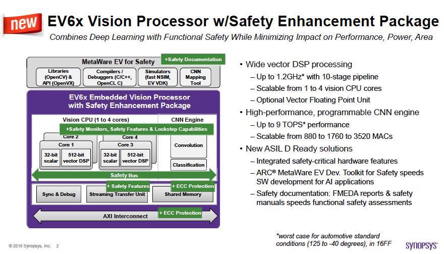
This joint CEVA and Open-Silicon webinar, moderated by myself, will elaborate on Narrowband IoT (NB-IoT) custom SoC solutions that are based on the CEVA-Dragonfly IP subsystem, and serve a wide range of cost- and power-sensitive IoT applications. Those joining the webinar will learn about the CEVA-Dragonfly NB1 IP subsystem, which pre-integrates the CEVA-X1 processor, optimized RF, baseband, and protocol software to offer a complete NB-IoT modem IP solution that can be extended seamlessly with GNSS and sensor fusion functionality.

Registration
Date: Tuesday, June 19, 2018
Time: 8 a.m. PST / 11 a.m. EST
Duration: 60 mins

The webinar will also address Open-Silicon’s NB-IoT custom SoC platform and software SDK, and how they enable customers to differentiate within the silicon with robust security and proprietary accelerator features with reduced risk, development schedule and cost.

The panelists will discuss the role of turnkey custom SoCs in lowering entry barriers, reducing time-to-market, increasing performance, adding security, and facilitating customization and scalability. The panelists will present sample use case platforms and explain how custom SoCs can enable product differentiation and total cost of ownership (TCO) savings for the next generation of NB-IoT applications.

This webinar is ideal for hardware designers and system architects of NB-IoT equipment/modules.

Speakers:

Emmanuel Gresset
Business Development Director, CEVA
Emmanuel is a Business Development Director in CEVA Wireless BU. For the last 30 years, Mr. Gresset has been with systems and semiconductor companies working in the fields of signal processing, wireless modems as well as processor and system-on-a-chip architecture in various companies: Octasic, STMicroelectronics, Philips, VLSI Technology, Spectral Innovations and Thomson. He received his M.Eng from the Ecole Supérieure d’Electricité in Paris.

Pradeep Sukumaran
Director, Systems & Software, Ignitarium
Pradeep Sukumaran is Director, Systems & Software at Ignitarium, a front-end design and software consulting company of Open-Silicon. Ignitarium offers high end VLSI and SW solutions to customers, with a strong focus on IoT and Vision Intelligence technology. Pradeep has over 17 years of experience in the embedded software and systems domain. Prior to Ignitarium, he was Senior Solutions Architect at Open-Silicon.

Naveen HN
Engineering Manager, Open-Silicon
Naveen HN is an engineering manager for Open-Silicon. He oversees board design, post-silicon validation and system architecture. He also facilitates Open-Silicon’s SerDes Technology Center of Excellence and is instrumental in the company’s strategic initiatives. He has over 16 years of experience in various domains of embedded systems design. Naveen is an active participant in the IoT for Smart City Task Force, which is an industry body that defines IoT requirements for smart cities in India. He received his M. Tech from SJCE, Mysore.

About CEVA, Inc.
CEVA is the leading licensor of signal processing platforms and artificial intelligence processors for a smarter, connected world. We partner with semiconductor companies and OEMs worldwide to create power-efficient, intelligent and connected devices for a range of end markets, including mobile, consumer, automotive, industrial and IoT. Our ultra-low-power IPs for vision, audio, communications and connectivity include comprehensive DSP-based platforms for LTE/LTE-A/5G baseband processing in handsets, infrastructure and machine-to-machine devices, advanced imaging and computer vision for any camera-enabled device, audio/voice/speech and ultra-low power always-on/sensing applications for multiple IoT markets. For artificial intelligence, we offer a family of AI processors capable of handling the complete gamut of neural network workloads, on-device. For connectivity, we offer the industry’s most widely adopted IPs for Bluetooth (low energy and dual mode) and Wi-Fi (802.11 a/b/g/n/ac/ax up to 4×4). To learn more, visit us at www.ceva-dsp.com

About Open-Silicon, Inc.
Open-Silicon transforms ideas into system-optimized ASIC solutions within the time-to-market parameters desired by customers. The company enhances the value of customers’ products by innovating at every stage of design — architecture, logic, physical, system, software and IP — and then continues to partner to deliver fully tested silicon and platforms. The company has partnered with over 150 companies ranging from large semiconductor and systems manufacturers to high-profile start-ups, and has successfully completed 300+ designs and shipped over 135 million ASICs to date. To learn more, visit www.open-silicon.com


ISO 26262 First – ASIL-D Ready Vision Processor IP Available

ISO 26262 First – ASIL-D Ready Vision Processor IP Available
by Tom Simon on 05-29-2018 at 12:00 pm

Synopsys made a pretty major announcement regarding their new ASIL-B,C and D ready embedded vision processor IP. This matters because you cannot bolt on the design elements and features needed to achieve these ASIL levels later, and this IP is absolutely necessary for ADAS systems and other critical safety systems in automobiles. These features have to be baked into the architecture, and the tools necessary to support them also need to be available. Simultaneously, Synopsys has gone to great lengths to ensure that the added safety features have minimal impact on performance.

So, what exactly are some of these features? Their press release itemizes them: “lockstep capabilities, ECC memories, error checking on core registers and safety-critical registers, a dedicated safety monitor, and a windowed watchdog timer for each core. An optional dedicated safety island monitors and executes safety escalations and diagnostics within the SoC and protects system bring-up”.

However, a list of safety features is not enough, there are a few more essential elements needed to crack the barrier to successfully implementing a vision processor based SOC for a system that complies with ISO 26262. Performance and capability are the first two major items to check off. The other necessary piece is development tools that are also ASIL ready. Let’s talk about these in order. I was fortunate enough to chat with Gordon Cooper, Product Marketing Manager at Synopsys for EV processors, about these topics. Much of what he discussed went beyond the press release and made it easier to understand their latest announcement.

Gordon told me that the crux of the announcement is that they have added the Safety Enhancement Package to their EV6x family of vision processors. Also, they have added vector processing that runs up to 1.2GHz with a 10 stage pipeline. The 1.2GHz speed, he pointed out, is at worst case for automotive standard conditions of 125 to -40 C in 16FF. Performance like this is much harder to achieve in these conditions, however they represent what is commonly found in automotive operating environments. Gordon emphasized that benchmarking for these applications is extremely important, it’s not enough to read a spec sheet and try to make a decision.

Gordon talked about data processing requirements for these systems as well. They are seeing 3-4 megapixel image sizes at frame rates of 30 fps, and increasing. By 2020 there will be over 24 cameras per vehicle as well as radar, all with higher resolutions. Yet, for different tasks, there needs to be differentiation in the kind of processor that is required. For instance, monitoring a driver’s face to detect distracted driving is a far different task than pedestrian or object detection. Synopsys offers different configurations of its EV6x family for each of these categories of tasks.

Gordon says that after thorough examination they have decided that 8 or 12 bit precision is preferred to the 16 bit precision often used. TensorFlow coefficients start out as 32 bit float, but they are quantized to 12 or 8 bits for recognition applications, with 8 bit being suitable in most instances.

On the tools side, they have invested in creating the documentation necessary to facilitate ASIL-D qualification. The tool chain has EV runtime and libraries, including OpenVX and OpenCV kernel libraries. They support C/C++ and OpenCL for developing applications and vision kernels. In addition, there is comprehensive debugging tool support. Synopsys also has a CNN graph mapping tool that helps mapping to the CNN engine. System level simulation support is available with system level models for host and EV processors.

Synopsys already has a large presence in the automotive market. Their processors are used in almost every application within that space. They already have customers who have taken some of the ASIL-D ready EV6x family to silicon. Availability of this IP will help accelerate ISO 26262 certification. Gordon also made it clear that they are going to be supplying their customers with a steady stream of updates to ensure they benefit from the latest research in vision processing. There is extensive material available on their website about the EV6x vision processor family and the Safety Enhancement Package that provides ASIL-D readiness.


Innovation in a Commodity Market

Innovation in a Commodity Market
by Bernard Murphy on 05-29-2018 at 7:00 am

Logic simulation is a victim of its own success. It has been around for at least 40 years, has evolved through multiple language standards and has seen significant advances in performance and major innovations in testbench standards. All that standardization and performance improvement has been great for customers but can present more of a challenge for suppliers. How do you continue to differentiate when seemingly everything is locked down by those standards? Some may be excited the potential for freeware alternatives; however, serious product companies continue to depend on a track-record in reliability and support, while also expecting continuing improvements. For them and for the suppliers, where do opportunities for evolution remain?

Performance will always be hot. Progress has been made on a bunch of fronts, from parallelism in the main engine (e.g. Xcelium) to co-modeling with virtual prototyping on one side (for CPU+SW) and emulation on the other (for simulation acceleration). However, I was struck by a couple of points Cadence raised in an SoC verification tutorial at DVCon 2018, which I would summarize as raw simulator performance only delivers if you use it effectively. Some of this comes down to algorithms, especially in testbenches. It’s easy to write correct but inefficient code; we’ve all done it. Being intelligent about limiting complex calculations, and using faster algorithms and better data structures, these are all performance optimizations under our control. Coding for multi-core is another area where we really shouldn’t assume tools will rescue us from ourselves. (You can check out the tutorial when these are posted by DVCon).

We can optimize what we have to repeat on each run. I’ve written before about incremental elaboration – rebuilding the simulation run-time image as fast as possible given design changes. Incremental compile is easy, but elaboration (where modules and connections are instantiated) has always been the bottleneck. Incremental elaboration allows for large chunks of the elaborated image to remain untouched while rebuilding just those parts that must be changed. Save/Restart is another widely used feature to minimize rework, since getting through setup can often take 80% of the run-time. However, this capability has historically been limited to understanding only the simulation model state. Now that we have test environments reading and writing files and working with external code (C/C++/SystemC), that basic understanding has limited checkpointing to “clean” states, which can be very restrictive. The obvious refinement is to save total model state in the run, including read and write pointers and the state of those external sims. Which you now can.

An obvious area for continued innovation is around AMS support, and one especially interesting domain here is power modeling in mixed-signal environments. This gets a little more complicated than in a digital UPF view since now you have to map between voltage values in the analog and power states in the UPF, among other things. The basics are covered in the standards (UPF and Verilog-AMS) but there’s plenty of room to shine in implementation. After all, (a) there aren’t too many industry-hardened mixed-signal simulators out there and (b) imagine how much power you could waste in mixed-signal circuitry if you don’t get it right. Cadence has notes on a few updates in this domain here, here and here.

X-propagation is another area related to power. Perhaps you thought this was all wrapped up in formal checks? Formal is indeed helpful in X-prop, but it can only go so far. Deep-sequence checks are obviously much more challenging, potentially unreachable in many cases. These problems are particularly problematic between (switched) power state functions. Missing isolation on outputs from such a function should be caught in static checks, but checking that isolation remains enabled until the block is fully powered up and ready to communicate, this ultimately requires dynamic verification.

However, there’s room to be clever in how this is done. Simulation can be pessimistic (always X when possible) or somewhat more optimistic, propagating only the cases that seem probable. Maybe this seems unnecessary; why not just code X’s into the RTL for unexpected cases? It seems the LRM can be overly optimistic (in at least some cases?), whereas X-prop handling through the simulator (no need to change the RTL) gives you more control over optimism versus pessimism. You can learn more about how Cadence handles X-prop in simulation here.

So yes, the innovation beat goes on, even in simulation, a true veteran of EDA. Which is just as well since it still dominates functional verification and is likely to do so for a long time yet 😎


China Chips Taiwan and Technology

China Chips Taiwan and Technology
by Robert Maire on 05-28-2018 at 12:00 pm

Three critical China issues; Trade, Taiwan & Technology. China is a “double edge sword” of risk & opportunity. These issues greatly impact stock valuations. We have recently given a presentation at both the SEMI ASMC conference in Saratoga Springs and The Confab conference in Las Vegas. Both conferences include senior management of the semiconductor industry covering a wide variety of topics.


For those who read our newsletter, you know we have opined on China and trade many times and of late the subject has come to the forefront of general news so this has turned out to be a very timely topic.

In our view it is very clear that the issue of China trade has at the very heart of it the semiconductor industry and can either negatively or positively impact the industry in a huge way. Investors and industry participants must pay particular attention to this issue as it has come to a head and the stocks and fortunes of the companies will be greatly impacted.

Right now we see more downside beta than upside. Just the mere threat of a trade war has likely changed the momentum in the relationship between China and the US for the negative. Over the last several weeks we have seen a rollercoaster ride of reversing directions in trade that has left everyone spinning and confused.

Technology is also at the heart of trade as who has the technology and who wants it and how they get it have huge implications. We have already seen some early warning signs of technology ownership issues.

Finally Taiwan has not been mentioned much but everyone seems to forget that Taiwan is a short missile flight away from China that has recently raised the Taiwan issue again by forcing airlines to name Taiwan as part of China. While this may seem petty, it is a more ominous message sent by China about the future of Taiwan and with it TSMC and all the semiconductor operations on the runaway island.

Below is a link to the slide deck of the presentation we have given as we think it will be of interest to investors and industry participants alike…

China Chips- Trade Taiwan & Technology

Conclusion: Resistance is Futile- Join the Movement!

*Much like Japan, Taiwan & Korea before them, China entering the semiconductor industry is a normal progression of modernization

*The US will also need alternative suppliers like Micron & GloFo

*The US can participate and profit in China – A huuuuge market

*Everyone must participate with eyes wide open to risks

*The US government can help level the playing field of trade & IP concerns

*China will likely be faster than Japan, Korea or Taiwan in build up

*US must promote & protect & invest in new tech – AI, VR, IOT etc…

*China remains a very sharp double edged sword that cuts both ways


Should EDA Follow a Foundry Model?

Should EDA Follow a Foundry Model?
by Daniel Nenni on 05-28-2018 at 7:00 am

There is an interesting discussion in the SemiWiki forum about EDA and the foundry business model which got me to thinking about the next disruptive move for the semiconductor industry. First let’s look at some of the other disruptive EDA events that I experienced firsthand throughout my 30+ year career.

When I started in 1984 EDA was dominated by what we called DMV (Daisey, Mentor, Valid). Before that it was Calma running on Data General Minicomputers. Back then EDA was a systems business where software was bundled with hardware. SUN Microsystems and Cadence changed that by putting minicomputers on engineer’s desks allowing them to pick and choose the software tools they used. EDA then became a software centric business selling perpetual licenses with yearly maintenance contracts. Software subscriptions soon followed which caused a bit of financial indigestion for EDA companies but clearly it was disruption for the greater good.

The most recent EDA disruption is Siemens acquiring Mentor. We are now seeing the effect it is having on the ecosystem, a very positive effect. We now have three VERY competitive EDA companies going upstream from chip to software development to complete systems. It really is an exciting time to be in EDA!

Meanwhile, back at the castle, the majority of commercial software is now in the cloud via an SaS business model resulting in gold mines of data and analytics, except of course EDA software.

The forum discussion Should EDA Follow a Foundry Model? was started by long time SemiWiki member Arthur Hanson. Arthur is a hardcore investor who came to SemiWiki looking for semiconductor knowledge to supplement his stock portfolio. Arthur and I have met, we talk on the phone and email. I was just starting to work with Wall Street at the time and found his investor insight quite helpful. Remember, when an outsider asks a question you need to understand what he is asking and why he is asking it.

“Just like asemifoundry takes knowledge in executing making chips for a variety of customers and shares it, yet keeps each customers information separate and private, should not an EDA firm be set up in its own cloud to share the expertise that they develop from monitoring a large number of separate process for different be used to improve the processes for all their customers? TSM has done an excellent job of keeping individual customer IP separate and private but uses the improvement in process information to the benefit of all. Would not this process if applied to EDA speed up the evolution of the design process to the benefit of all through the use of big data. If TSM can keep proprietary information separate and confidential while spreading process improvements, couldn’t EDA firms use the same structure to benefit their customers as well. Auditing the process on a real time basis could assure security while giving the customer the best practices on a real time basis. This could also be done on a virtual machine bases with most of the process done at the customerssite, although this would be unwieldy and cumbersome compared to a private cloud. Any thoughts, comments or observations on this appreciated and solicited.”

The resulting discussion is quite interesting so check it out when you have time. More than five thousand people have viewed it thus far which is a pretty big discussion if you think about it, and I have. SemiWiki is made up of all levels of semiconductor professionals from A to C level and we know who reads what, when, and where, so I can tell you this discussion is resonating at all levels of the ecosystem, absolutely.

My personal opinion is that disruption is again coming to EDA and that disruption will be in the cloud. We did a “Do you want your EDA Tools in the cloud” poll and again the interesting part was who voted and where they were in the ecosystem. The $10B question is: Who is trusted enough to implement EDA in the cloud? The answer is towards the end of the forum discussion:

Originally Posted by count
I think it would be interesting if the foundries, ie TSMC, got into the EDA game and charged a wafer royalty on it as you said. Better yet, a cloud based EDA tool that could also be used for ordering after designs are validated. If it could be integrated in a sort of design to manufacturing workflow, that would be amazing. Especially for smaller customers who are designing IoT chips and are focused on time to market, something like that seems like it could be valuable.

Originally Posted by KevinK
Why would a TSMC or Samsung even consider this option given Cadence’s or Synopsys’ current market caps and revenues ? Given the stock premium that an acquisition would cost, either foundry could build two leading edge fabs for the same price. I don’t know Samsung’s internal economics, but TSMC’s typical return on invested capital (ROIC) runs around 30-40%. Even though an EDA acquisition wouldn’t be “capital” per se, I’m sure that the foundries would use their ROIC as a hurdle rate for other major uses of money. Neither EDA company offers close to that rate, even before considering the revenue haircut an EDA/IP company would suffer, once tied to a single foundry.

Originally Posted by Daniel Nenni
One word: Disruption
Do you actually think Intel Foundry or Samsung Foundry or any other IDM foundry for that matter has a chance at catching up with TSMC while playing by TSMC’s rules? Much less beating them? It’s not gonna happen. Intel or Samsung could buy Cadence or make a significant investment and cut a wafer royalty deal in the cloud exclusive to their customers. Foundries, better than EDA companies, could pull of EDA in the cloud, absolutely.

Just my opinion of course…


Dear Toyota

Dear Toyota
by Roger C. Lanctot on 05-27-2018 at 7:00 am

Toyota Motor North America CEO James Lentz got a letter from the U.S. Federal Communications Commission (FCC) last week recognizing Toyota’s announced plan to deploy Dedicated Short Range Communications (DSRC) technology on Toyota and Lexus vehicles sold in the U.S. beginning with MY21. The extraordinary letter notes that Toyota’s decision comes 20 years after the FCC allocated spectrum for DSRC technology, but cautions that Toyota ought to weigh such significant capital investments against the emergence of superior competing solutions, most notably cellular-based C-V2X.
Continue reading “Dear Toyota”


China Semiconductor Equipment China Sales at Risk

China Semiconductor Equipment China Sales at Risk
by Robert Maire on 05-27-2018 at 7:00 am

We have been on a roller coaster ride of on again off again trade talk between China and the US. It is unclear where we are on a day by day basis but of late it appears that we are not seeing a lot of progress and some progress we thought we had made may not have actually happened.
Continue reading “China Semiconductor Equipment China Sales at Risk”


Webinar: IP Quality is a VERY Serious Problem

Webinar: IP Quality is a VERY Serious Problem
by Daniel Nenni on 05-25-2018 at 12:00 pm

We just completed a run through of the upcoming IP & Library QA webinar that I am moderating with Fractal and let me tell you it is a must see for management level Semiconductor Design and Semiconductor IP companies as well as the Foundries. Seriously, if you are an IP company you had better be up on the latest QA checks if you want to do business with the leading edge foundries and semiconductor companies, absolutely.


The secret weapon here is presenter Felipe Schneider, Director of Field Operations at Fractal. Felipe will take us through the agenda followed by a demonstration of Crossfire, ending with questions and answers. Felipe is the frontline interface to Fractal customers in North America which includes many of the top semiconductor companies and IP providers so he knows IP QA. Felipe also knows what QA checks are being done at the different process nodes down to 7nm and what new checks are coming at 5nm (crowdsourcing). This alone is worth an hour of your day.

IP & Library QA with Crossfire: Wed, Jun 6, 2018 9:00 AM – 10:00 AM PDT

There is no industry where the need for early bug detection is more paramount than in SoC design. Consequences like design re-spins, missed tape outs and hence missed market opportunities make the cost of late bug detection prohibitive. Where earlier generations of SoC designs could be crafted by a team of limited size that could oversee the entire design process, design in the latest process nodes requires a different strategy.

Designer productivity is lagging behind Moore’s law which drives the increase of transistor density. Thus design teams are becoming larger and are comprised of multiple groups spread over the globe. Outsourcing of design tasks by integrating third-party IP is mandatory to get the job done, but it reduces oversight of the SoC design process and leaves companies at the mercy of the quality strategy implemented by their suppliers. At the same time, modelling of new physical effects using current-driver, variation and electro-migration models paired with an increased amount of PVT corners generate an explosion of data to be analyzed prior to sign-off.

It is clear that QA needs to be a shared responsibility by all partners in the SoC design flow, from library and IP providers to foundry and SoC integrators. Each of these partners needs an integrated QA solution in their part of the design flow. Never should QA be an afterthought to be checked off right before IP delivery. This webinar intends to cover how Fractal Technologies Crossfire solution addresses these QA challenges from both backend and frontend perspectives and why its standardized and scalable QA methodology is superior to homebrew validation solutions.

About Crossfire
Mismatches or modelling errors for Libraries or IP can seriously delay an IC design project. Because of still increasing number of different views required to support a state of the art deep submicron design flow, as well as the complexity of the views themselves, Library and IP integrity checking has become a mandatory step before the actual design can start.

Crossfire helps CADS teams and IC designers in performing integrity validation for Libraries and IP. Crossfire makes sure that the information represented in the various views is consistent across these views. Crossfire improves Quality of your Design Formats.

About Fractal Technologies
Fractal Technologies is a privately held company with offices in San Jose, California and Eindhoven, the Netherlands. The company was founded by a small group of highly recognized EDA professionals.


Welcome DDR5 and Thanks to Cadence IP and Test Chip

Welcome DDR5 and Thanks to Cadence IP and Test Chip
by Eric Esteve on 05-25-2018 at 7:00 am

Will we see DDR5 memory (device) and memory controller (IP) in the near future? According with Cadence who has released the first test chip in the industry integrating DDR5 memory controller IP, fabricated in TSMC’s 7nm process and achieving a 4400 megatransfers per second (MT/sec) data rate, the answer is clearly YES !

Let’s come back to DDR5, in fact a preliminary version of the DDR5 standard being developed in JEDEC, and the memory controller achieving a 4400 megatransfers per second. This means that the DDR5 PHY IP is running at 4.4 Gb/s or quite close to 5 Gb/s, the speed achieved by the PCIe 2.0 PHY 10 years ago in 2008. At that time, it was the state of the art for a SerDes, even if engineering teams were already working to develop faster SerDes (8 Gb/s for SATA 3 and 10 G for Ethernet). Today, the DDR5 PHY will be integrated in multiple SoC, at the beginning in these targeting enterprise market, in servers, storage or data center applications.

These applications are known to always require more data bandwidth and larger memories. But we know that, in data center, the power consumption has become the #1 cost source leading to incredibly high electricity bill and more complex cooling systems. If you increase the data width for the memory controller while increasing the speed at the same time (the case with DDR5) but with no power optimization, you may come to an unmanageable system!
This is not the case with this new DDR5 protocol, as the energy per bit (pJ/b) has decreased. But the need for much higher bandwidth translates into larger data bus width (128-bit wide) and the net result is to keep the power consumption the same as it was for the previous protocol (DDR4). In summary: larger data bus x faster PHY is compensated by lower energy/bit to keep the power constant. The net result is higher bandwidth!

You have probably heard about other emerging memory interface protocols, like High Bandwidth Memory 2 (HBM2) or GraphicDDR5 (GDDR5) and may wonder why would the industry need another protocol like DDR5?
The answer is complexity, cost of ownership and wide adoption. It’s clear that all the DDRn protocols, as well as the LPDDRn, have been dominant and saw the largest adoption since their introduction. Why will DDR5 have the same future as a memory standard?

If you look at HBM2, this is a very smart protocol, as the data bus is incredibly wide, but keeping the clock rate pretty low (1024 bit wide bus gives 256 Gbyte/s B/W)… Except that you need to implement 2.5D Silicon technology, by the means of an interposer. This is a much more complex technology leading to much higher cost, due to the packaging overcost to build 2.5D, and also because of the lower production volume for the devices which theoretically lead to higher ASP.

GDDR5X (standardized in 2016 by JEDEC) targets a transfer rate of 10 to 14 Gbit/s per pin, which is clearly an higher speed than DDR5, but requires a re-engineering of the PCB compared with the other protocols. Sounds more complex and certainly more expansive. Last point, if HBM2 has been adopted for systems where the bandwidth need is such than you can afford an extra cost, GDDR5X is filling a gap between HBM2 and DDR5, this sounds like the definition of a niche market!

If your system allows you to avoid it, you shouldn’t select a protocol seen as a niche. Because the lower the adoption, the lower the production volume, and the lower the competition pressure on ASP device cost… the risk of paying higher price for the DRAM Megabyte is real.

If you have to integrate DDR5 in your system, most probably because your need for higher bandwidth is crucial, Cadence memory controller DDR5 IP will offer you two very important benefits: low risk and fast TTM. Considering that early adopters have already integrated Cadence IP in TSMC 7nm, the risk is becoming much lower. Marketing a system faster than your competitors is clearly a strong advantage and Cadence is offering this TTM benefit. Last point, Cadence memory controller IP has been designed to offer high configurability, to stick with your application needs.

From Eric Esteve (IPnest)

For more information, please visit: www.cadence.com/go/ddr5iptestchip.


Managing Your Ballooning Network Storage

Managing Your Ballooning Network Storage
by Alex Tan on 05-24-2018 at 12:00 pm

As companies scale by adding more engineers, there is a tendency to spread across multiple design sites as they strive to hire the best available talent. Multi-site development also impacts startups as they try to minimize their burn rate by having an offsite design center such as India, China or Vietnam.

Both the IoT and automotive companies are becoming dependent on 5G and AI as their key drivers, fueling trend for more heterogeneous design projects. At the heart of this increased design collaborations of multiple companies across different sites is the necessity of addressing how design data creations, sync-ups and handoffs are done. We will look into some critical success factors in this area and discuss their available solutions.

EDA flows and design teams
A typical design flow begins when RTL is developed for a specific design specification and then synthesized to gate level, followed by placement optimization, clocking, routing and parasitic extraction intended for timing signoff. It is common to have many process owners across these implementation stages. Once design development started, each designer tends to copy the entire project data into their workspace and annotated their works to propagate further the design realization closer to layout.

The process gets iterated multiple times, some with smaller loops such as in performing localized placement changes and redoing the route, while others may cover many steps such as doing ECOs, or even may trigger a loop-back to the starting point (for example when upstream input files such as RTL version, tool version or run settings change). During each of these events, more design data get duplicated, ballooning up the design data usage (refer to figure 1a).

In addition, early design targets such as the libraries, developed foundation and design IPs that absorb new technology specifications and precede a system design implementation are subjected to frequent version refresh, triggering downstream updates of design implementation cycle and eventually more large data duplication.

Many instances, temporary measures such as local compression with gzip or tarz commands is attempted as designer has limited time to wrestle with the growing design data. This could become a nuisance and still does not prevent data duplication issue.

A hardware configuration management solution such as ClioSoft SOS7 resolves some of the issues faced with the ballooning network storage by greatly simplifying access to the real time database and efficiently managing the different revisions of the design data during design development as illustrated in figure 1b.

It enables distributed reference and reuse through the use of primary and cache servers. Both servers provide controls for a comprehensive data management across sites, enabling effective team collaboration by allowing data transparency and reducing data duplications. Any design team has several team members who need constant access to certain parts of the design data. SOS7 enables better automation by providing for the notion of a configuration wherein designers can access the necessary files based on the role they play in the team. While this improves the disk space usage by preventing copying unwanted files, it also adds a layer of security by limiting access to all files. It has seamless integration with many other EDA flows and allows GUI driven customization for designers to browse libraries and design hierarchies, examine the status of cells, and perform revision control operations without leaving the design environment or learning a new interface.

Usage of network storage

Design development usually starts with one or two shared disk partitions typically ranging from over hundred to 250Gb. Over several project integration snapshots, new additions to the team and several implementation stages, the network storage assigned to the project could easily reach to several terabytes size. At this stage, design teams often resort to segregating team data into cluster of disks such as for front-end, backend, verification –which may address ownership or usage tracking but does not address the main issue of managing the ballooning network storage usage (figure 2a).

Network storage also grows because of the reluctance of the engineers to discard what is perceived as unwanted data. Most data has a lifespan and becomes irrelevant after some time but both project manager and designers tend to retain most of the generated data including those intermediate ones, until a stable results could be achieved.

The cost of maintaining project data footprint is not limited to supporting the given workarea capacity, but also in providing redundant builds by IT for backup purposes. The growing number of physical disk partitions also affects the overall data access performance and IT maintenance efforts as mountable disks recommended threshold could be exceeded.

The solution
ClioSoft’s SOS7 design management platform addresses the issue of managing the ballooning network by using smartlinks-to-cache to link files which have populated the workareas. All directories and files are essentially treated as symbolic links which ensures that the workspace population is fastly accessible and with minimal disk space usage (illustrated in figure 2b, 2c).

This becomes especially useful when the binaries are large and coupled with a big design hierarchy. It is a key solution metric as other SCM solutions that do not take care of this has to deal with text files –and solutions built on top of these SCMs have to use either hardware solutions or make modifications to the file system to achieve network storage space savings

SOS7 has been architected to ensure high performance between the main server and the remote caches. Any time a user wants to modify the file or a directory, it is quickly dowloaded from the local cache or the main repository with minimal download time. SOS7 also provides for the notion of a composite object which manages a set of files as one entity.

When running the EDA software, a number of files are generated, some of which change with each run. Designers often like to keep the generated data from multiple runs as it enables them to compare the results and revert back to the previous design state if needed. SOS7 manages these files efficiently by treating the generated files as a composite object –without duplicating any files which do not change with each run of the EDA tool– thereby providing the designers with the flexibility they desire and at the same time minimizing the network usage space.

Disk space cost
Measuring disk space costs in dollars per gigabyte only covers half of the equation. One needs to consider additional cost drivers and dispel the common myth about storage total cost of ownership based on total capacity. For example, overhead attributed to reduced capacity due to derating, array-based redundancy and the file system coupled with cost needed for power, cooling and floorspace –all could add between 40-70 percent more on the cost.

Other challenges include the need to provision separate storage systems for data backup. All of these disk capacity demand is becoming prohibitive as limited budget constraint is usually imposed on a project. Hence, resolving network space usage at its root, that is an efficient data creation and management should help ensure adequate project storage capacity and performance.

ClioSoft SOS7 delivers features addressing such a need through enabling design dependencies reuse (such as flexible project partitioning including IP and PDKs), a comprehensive version control mechanisms (such as support to project derivative creation through branching) and previously discussed composite-object referencing.

For more info on SOS7 case studies or whitepaper, click HERE.

Also Read

HCM Is More Than Data Management

ClioSoft and SemiWiki Winning

IoT SoCs Demand Good Data Management and Design Collaboration