EDA companies advertise their physical verification tools, aka DRC (Design Rule Check), mostly in terms of specific engine qualities such as capacity, performance and scalability. But they do not address an equally if not more important aspect: the correctness of the actual design rules.
Put bluntly: It’s not about how fast you check, it’s about what you check. To draw an analogy from a slightly different EDA domain: Designers can implement their RTL design in an FPGA device from vendor-A or vendor-X. Sure, there are differences between the two, but in essence, if the logic circuit fits in both devices and they are fast enough, either will do. What absolutely cannot be compromised is the correctness of the RTL code. If there are bugs in the RTL code, extra capacity and higher speed of the FPGA device will not help; functional verification is of the essence.
DRC is all about the runset
The same holds for DRC. One tool may run faster or take less memory than the other, but in the era of abundant and low cost cloud computing these are not critical factors any more. The quality of the check is determined less by the engine that runs it, and more by the correctness of the DRC runset code:
- Is the DRC runset code correct? : Does it accurately represent the design rule intent?
- Are the rule checks complete? : Does the DRC code cover all possible layout configurations?In practice the likelihood and severity of potential issues vary from case to case; broadly one can distinguish between the following three situations:
- A physical design that is implemented in a mature technology that “saw” hundreds or thousands of designs already. In this case chances are that “holes” and bugs have already been (painfully) found in previous designs and have been fixed by the foundry. Using a 5-years-in-volume-production vanilla flavor process? – probably no need to worry.
- A design that targets a relatively new technology, or a customized process flavor. There is a reasonable chance that the runset may still have inaccuracies or hidden “holes”. In this case it makes sense to inquire about the QA process of the runset, how many different designs have used the exact same process in production. If some design rules are customized and specific for this product or design style – runset verification can save a lot of cost and grief.
- An early technology project: be it a foundry internal technology enablement project, an IP partner project, or an early access customer design team working closely with the foundry. In this case the runsets are clearly work in progress and must go through rigorous verification and QA process.The next obvious question is what tools and methodologies are available to address these issues and verify the DRC runset?Runset verification with DRVerify
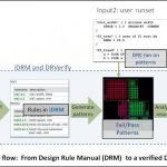
DRVerify is the leading commercial tool for DRC runset verification. Here is why: - Spec driven: The tool reads the foundry design rule descriptions (from any spreadsheet or text file) and allows to enter rules using a GUI. This rule description that represents the rule intent and is independent of a particular implementation is the source for creating the tests and the reference for their correctness and accuracy.
- Powerful enumeration: DRVerify has a pattern enumeration engine then automatically generates pass/fail variations that exercise all boundary conditions of each design rules. The generated fail and pass cases cover all situations based on the design rule description (spec).
- Flexibility: In addition to the automatic layout creation, the tool accepts additional layout patterns or actual design clips. Given such clips, the tool will automatically recognize the rules under test, and use them as seeds for further pattern enumeration.
- The tool uses an internal independent spec-driven DRC engine that examines all these test cases, sorts them into fails and passes and places markers that are later compared to the markers created by the target DRC tool runset.
- Coverage: DRVerify has a coverage measurement engine that analyzes all fail/pass cases and determines the level of coverage accomplished for each rule.
- Detailed error report: Once the target runset or DUT (deck under test) runs on the QA test layout, DRVerify will run a comparison between each DUT marker and its own markers and measurements, and will provide a detailed comparison report, pointing to any mismatch or potential error in the runset.
- No limitations: DRVerify is not limited to any given set of rules or specific technologies.
- Tool independence: DRVerify is tool agnostic and can be used to verify any runset for any DRC tool or language.To learn more about DRVerify: DRVerify White Paper