webinar banner AI 2026 v2

Meeting Automotive IC Design Challenges for Safety using On-Chip Sensors

Meeting Automotive IC Design Challenges for Safety using On-Chip Sensors
by Daniel Payne on 05-09-2019 at 7:00 am

I’ve been driving cars since 1978 and have even done a few DIY repairs in the garage, so I know how warm the engine compartment, transmission or exhaust system can become which makes automotive IC design rather unique in terms of the high temperature and voltage ranges that an electronic component is subjected to. Our safety while driving a car is paramount, so automotive designers have a big responsibility to manage the electronic subsystems that are hidden from view. Recent advances in ADAS (Advanced Driver Assistance Systems) by the major automotive companies along with EV startups like Tesla, are also adding an unprecedented number of ICs and sensors like RADAR and LiDAR to our vehicles.


ADAS Features. Source: Robotics & Automation

Ideally then, at the chip-level, your designers would like to know what the Process variation, Voltage levels and local Temperatures (PVT) are so that they can control the chip operation, keeping it operating safely and within specifications, instead of failing from heat-induced electromigration failures or supply voltages out of spec. Let me just summarize some of the automotive IC design challenges:

  • Reliability
  • Adherence to standards like ISO 26262
  • Long term commitment from suppliers
  • Monitoring aging effects
  • Drift
  • Safety
  • Long development cycles

ISO 26262. Source: National Instruments

ITRI Industrial International forecasts an 11.9% annual growth rate for automotive electronics from 2017 to 2022, so that has the IC design community highly motivated to design new chips to meet the challenges of ADAS. On the infotainment side our cars are becoming mobile hotspots, enabling us to enjoy non-stop smart phone use along with new ways of controlling the car dashboard with our voice or touching a screen.

Chips inside of cars can use bleeding edge 7nm silicon from Samsungor TSMC, all the way up to mature 180nm nodes. The smaller the node, the greater the impact of process variation has on the reliability. If you knew which process corner each block was operating under, then you could take design steps to control the frequency and voltage levels in order to stay within your power spec for example.

Thermal effects continue to be important for automotive ICs:

  • FinFET structures are less able to dissipate heat than planar CMOS
  • Increased density is leading to increased thermal challenges
  • Electrical OverStress (EOS)
  • Electromigration (EM)
  • Hot carrier aging
  • Increased Negative Bias Temperature Instability (NBTI)
  • Device leakage causes heat and heat causes more leakage (Thermal runaway)
  • Leakage to increase when we move from one FinFET node to the next smaller node

Ashish Kumar Gupta from Freescale Semiconductors summarizes thermal concerns, “Designers face new challenges of providing thermal-efficient systems that balance or equally distribute possible on-chip hot spots. In this scenario, Dynamic Temperature Management (DTM) techniques arise as a promising solution. DTM relies on accurately sensing and managing on-chip temperature, both in space and time, by optimally allocating smart temperature sensors in the silicon.

Fortunately for new chip designs targeted at automotive you don’t have to create your own semiconductor IP for PVT monitoring, because there’s a vendor focused solely on PVT monitoring fabrics, Moortec. They are members of the TSMC IP Allianceand have over a decade of experience in this domain. Their in-chip monitoring subsystem IP is silicon proven at 40nm, 28nm, 16nm, 12nm and 7nm, so that’s a wide range to choose from. In addition the IP that Moortec supplies to TSMC users has passed the rigors of the TSMC9000 quality program.


Source: TSMC

Engineers want to know how all of the pieces fit together for IP, so here’s a diagram that shows the concept of connecting multiple PVT monitors and a subsystem to control them.


PVT Sub-system

For automobiles the environmental temperature range is typically -40C to 125C, but the junction temperature of the IC is going to be even hotter than 125C worst case based on the number of transistors, process node, operating frequency and voltage levels. Having multiple Temperature monitors on-chip is a wise choice in managing the thermal specification. As a chip reaches its thermal limits then the control logic can be used to lower voltage levels, decrease frequency or a little of both.

As IC designers identify thermal hotspots in the layout, then engineers can judiciously place Thermal monitors around the chip in order to measure junction temperatures in realtime, then take corrective action when needed.

Summary
The process variation, voltage variation and thermal challenges of designing automotive ICs can be met by placing multiple PVT monitor IP blocks as a fabric across your chip. Moortec is the leader in PVT monitoring subsystems from 40nm through 7nm nodes and has plenty of silicon proven results and use case experience, so that you can quickly use their IP and control how your chips react to variations, keeping them safe and operating within spec.

Related Blogs


eSilicon ASICs all in the Google Cloud

eSilicon ASICs all in the Google Cloud
by Daniel Nenni on 05-08-2019 at 12:00 pm

Having just completed a cloud evaluation for SemiWiki I can tell you why eSilicon chose Google. Simply put, they are working harder to get cloud business. Google ($4B) is the number five cloud provider behind Microsoft ($21.2B), Amazon ($20.4B), IBM ($10.3B) and Oracle ($6.08B). There is a lot of money in the cloud and a lot more to come which is why cloud providers are designing their own chips and partnering with ASIC providers like eSilicon to get that competitive edge. Speaking of ASICs in the cloud:

eSilicon Signs Multi-Year Agreement with Google Cloud
Under the terms of the agreement, Google Cloud will provide support from their professional services team to assist eSilicon as it moves its ASIC and IP design workloads to GCP. eSilicon has been running a hybrid on-premise/cloud environment for approximately the last 18 months, with ASIC design running on premise and IP design running primarily on GCP. This new agreement paves the way for a complete migration of all design activity to GCP.

“Google Cloud has demonstrated the resources, technical depth and domain knowledge to successfully move IC design to GCP, a significant undertaking,” said Naidu Annamaneni, CIO & vice president of global IT at eSilicon. “There are many unique requirements to support this kind of workload on the cloud and the need to collaborate with several infrastructure vendors to create the complete solution. Google Cloud possessed the domain knowledge and operational focus, backed by a substantial worldwide computing capability to get the job done.”

“Moving to the cloud provides the flexibility to build the right compute environment for each design project, resulting in improvements in time-to-market and design quality,” said Mike Gianfagna, vice president of marketing at eSilicon. “This is a substantial project with a lot of innovation and many partners. We’ll be talking more about this fast-paced program at it unfolds over the coming months.”

The big news here is that eSilicon is committing to move ALL ASIC and IP design to the Google Cloud Platform (GCP). They have been operating in a hybrid cloud environment for about a year and a half and now they are taking the next big step. Most of the chip design cloud activity today is hybrid so eSilicon is blazing trails here.

When it’s all said and done, there will be very few computers left inside eSilicon with all major infrastructure served in a flexible, cost effective, and highly secure way with GCP. Cost and security is critical but it’s the flexibility that makes the cloud a no-brainer for chip designers.

Remember, chip design is spiky in regards to compute resources. Processor speed, memory and storage requirements can vary a great deal, especially during the tapeout phase. There is no way an on-premise server farm can be competitive with a cloud offering during a tape-out. eSilicon can now apply the required compute resources needed to meet schedules, perform rigorous verification and deliver world-class ASICs. This ability to apply massive compute resources only when needed is unique to the cloud. The result is a higher quality design and all-important first-time-right silicon which is a make-or-break for the ultra competitive ASIC business.

The downside of the cloud is that you get what you ask for so you had better be careful what you ask for. For example, SemiWiki cloud resource requirements are easily predicted. Google cloud load balancing is as simple as adding a CPU, memory, or disk in a matter of clicks. eSilicon on the other hand is applying machine learning algorithms for an intelligent orchestration layer that assesses the need of a specific design project in regards to compute resources. It also manages costs based on project budgets from IP to full chip design. Expert resource management is a normal part of the ASIC business but with ML and the cloud it will be a completely different type of business, absolutely.

AbouteSilicon
eSilicon provides complex FinFET ASICs, market-specific IP platforms and advanced 2.5D packaging solutions. Our ASIC-proven, differentiating IP includes highly configurable 7nm 56G/112G SerDes plus networking-optimized 16/14/7nm FinFET IP platforms featuring HBM2 PHY, TCAM, specialized memory compilers and I/O libraries. Our neuASIC™ platform provides AI-specific IP and a modular design methodology to create adaptable, highly efficient AI ASICs. eSilicon serves the high-bandwidth networking, high-performance computing, AI and 5G infrastructure markets. www.esilicon.com


Anirudh Keynote at CDNLive 2019

Anirudh Keynote at CDNLive 2019
by Bernard Murphy on 05-08-2019 at 7:00 am

Anirudh Devgan (President of Cadence), gave the third keynote at CDNLive Silicon Valley this year. He has clearly become adept in this role. He has a big, but supportable vision for Cadence across markets and technologies and he’s become a master of the annual tech reveals that I usually associate with keynotes.


Anirudh opened with factors driving system design across major verticals: aero and defense, datacenters, mobile, auto and industrial. These drive trends in distributed and cloud-computing, 5G and edge computing (5G, recently a future, is catching up fast), automotive and industrial disruption, machine learning and deep learning. And in support of all this, the need for more complete optimization across systems, and always improving design excellence and productivity.

Cadence is organizing its approach to these new opportunities through SDE (System Design Enablement) 2.0, a three-level attack through support of design excellence (EDA and IP), System Innovation (a new area) and Pervasive Intelligence (also a new area). All of this leverages Cadence core-competence in computational software, the CS plus math expertise that underlies most EDA technologies. To Anirudh this is very important; Cadence needs to build and grow around existing core-competencies. Since a lot of system analysis requires computational software, as does ML, these are reasonable directions.

This requires a larger view of systems design because customers in all of these markets are now expecting to optimize complete systems, down into the chip/multi-chip design. It also requires an expanded view of computation, embracing the rapid ascendance in support of and use of AI technologies. This doesn’t mean that investment in “conventional” EDA takes a back seat. At the more advanced process nodes, tools must continue to progress in capability. Performance, and coupling with foundries becomes even more essential.

Stepping back for a second from new and shiny stuff, Anirudh had to toot Cadence’s (and his) horn on the dominance of the Cadence digital flow – 20% better PPA than alternatives in the full flow and over a hundred 7nm tapeouts.

Back to the new stuff, first Machine Learning. Anirudh breaks this up into Inside (ML inside a tool), Outside (eg. ML optimizing a flow for improved PPA) and Enablement (eg the support for customer ML objectives through the Tensilica IP). As examples of Inside, a tool looks more or less the same to a user but runs faster or delivers a better result; he cited Tempus as an example where these capabilities are already available.

An example of Outside ML is an iterative flow around Genus and Innovus, using learning gained through earlier runs to improve subsequent runs. Cadence has shown cases where they can get improvement in TNS of 10-20% using such flows. A somewhat different example is use of ML in optimizing PCB automated routing in Allegro where design times can be significantly reduced.

In System Innovation, one of Anirudh’s big reveals was the Clarity 3D solver, from die to package and system. I won’t spend much time on this because Tom Simon wrote about Clarity earlier, but some of the use-cases Anirudh cited may be new – an automotive application with LPDDR4, package, PCB and DIMM connector, a datacenter application for a 112G connection from server to cable to server, and a 5G handset application analyzing fanout wafer-level packaging through 40 DDR signals and power. All of this of course in distributed (and elastic) compute. Anirudh cited this as a good example of leveraging core expertise – building on Cadence know-how in solving matrices – not a skill you would find among most big-data experts.

The other big systems initiative is the partnership with Green Hills software; Anirudh noted that this has Cadence starting to play a role in a $4.5B system analysis market. Coupling that expertise together with early software bring-up and debug on the Palladium and Protium platforms enables analysis and optimization to move into pre-silicon design and further supports the total system objective that so many of the verticals are now finding essential.

I for one am eager to see support of electronic design expand beyond the narrow bounds of package and board and embrace at least some of the latest and greatest trends in tech. We need to play a bigger role in applications innovation. Cadence certainly seems to be taking some interesting steps in that direction.


When Artificial Intelligence Becomes Emotionally Intelligent

When Artificial Intelligence Becomes Emotionally Intelligent
by Krishna Betai on 05-07-2019 at 12:00 pm

“AI is the biggest risk we face as a civilization.” Words from the visionary Tesla CEO, Elon Musk. After each iteration of innovation, artificial intelligence edges closer to replicating the human brain; people fear that AI would soon steal their jobs, which has already started happening in some parts of the world. Yet, humans can take solace in the fact that they are ahead of AI-powered robots in one sphere—emotions.

The process that humans follow to complete a given task is strikingly similar to what AI does—identify data, analyze data, interpret the analysis, identify a suitable course of action, and implement that action. Consequently, the jobs of personal assistants, drivers, delivery persons, factory workers, financial analysts, and even doctors are endangered, along with the hundreds of jobs that involve clerical work. Moreover, there is only so much a human being can learn; AI has the upper ground in that there is no limit to what it can learn. If it runs out of memory, a new server comes to its rescue; there is no stopping the increase in its processing power.

Even though the smartest minds in the world strive to make AI smarter by adding more neural networks and feeding it volumes of data, it is unable to express emotion. It’s not surprising that the next avenue for artificial intelligence to explore is emotional intelligence. An Alexa that can laugh, a Google Assistant that can feel sympathy, a Siri that can admit its mistake and ensure to never do it again. What if artificial intelligence had emotional intelligence?

While AI can become the cause of employee redundancy in various industries due to its superior data processing capabilities and hard skills, humans are at an advantage for their emotional processing capabilities and soft skills, two things that they can hold onto proudly. Some tasks require more than just analyzing data and coming up a solution, these jobs demand a human touch. For example, a robot cannot take the place of a psychologist, who has to dive deep and understand the emotions and problems of a patient and offer tailored solutions and suggestions that might improve the patient’s mental health, although gradually. Only a manager in the form of a human being can motivate their team, tackle individual issues and conflicts and instill in them a sense to perform better and achieve greater results.

For artificial intelligence to develop emotional intelligence, it would need to understand a variety of complex emotions that requires more than simple data processing. If this did happen, having conversations with AI would result in more natural, human responses instead of robotic replies. It would take a considerable amount of time for human beings to open up to emotional artificial intelligence, for obvious reasons. A personal robot assistant with an emotional quotient would advise their boss against taking any stress during situations that emulate that feeling. Along with giving the perfect tactical instructions to the players of a sports team, emotional AI could motivate them by giving a pep talk, or even talk to players one-on-one.

There are a few instances where AI has slowly started developing emotional intelligence. The Google Assistant apologizes every time it makes an inadvertent mistake and acknowledges our appreciation when it performs a task with perfection. Amazon’s Echo for Kids communicates with children in a way that elders would, encouraging them to say “please” and “thank you”, suggesting that they should talk to their parents, siblings, or elders about sensitive subjects such as bullying, and even giving them leeway by recognizing “Awexa” instead of the usual name.

Emotional AI has a lot of potential in the real world. Humans are biased and can be judgmental at times, which is discouraging and even frightening for some who are too scared to vent their feelings. Emotional AI, with all its capabilities, can offer a safe haven for the people who find it difficult to express their emotions. A glimpse of this is shown in HBO’s sitcom Silicon Valley, in Episode 5 of Season 5, titled “Facial Recognition”. The protagonist, Richard, expresses his frustrations and feelings of jealousy toward a coworker to a robot named Fiona. The robot then sympathizes with Richard using its “emotional recognition protocol,” which helps it to identify a wide range of emotions including anger, anxiety, humility, entitlement, and self-loathing, to name a few.

However, AI with an emotional quotient could have potential downsides. The HBO sitcom covers this issue too when the robot analyzes its relationship with its creator, which is shown to be unhealthy and unprofessional and sends Richard an SOS message asking to be saved. In the next episode, “Artificial Emotional Intelligence,” Jared, a member of Richard’s team, develops an emotional attachment with the robot and is devastated when Fiona is torn apart for safety reasons.

Sure, emotional AI can help robots understand humans better, but there remains a possibility that humans can get emotionally attached to them and lose sight of reality. Or even worse, what if emotionally-intelligent robots realized how they are treated and turn against humans in an uprising?


Design IP in 2018: Synopsys and Cadence Increase Market Share…

Design IP in 2018: Synopsys and Cadence Increase Market Share…
by Eric Esteve on 05-07-2019 at 7:00 am

…but ARM, Imagination, MIPS or Ceva have declined and lose market share. Semiconductor design IP market is still doing good in 2018, with 6% growth year over year. It’s half the growth rate seen in 2017, 2016 and 2015 and the growth decline is imputable to bad results from ARM, the market leader, but also from Imagination (#4), MIPS (#10) or CEVA (#5).

In fact, 2018 was an excellent year for #2 Synopsys (+19.4%) or #3 Cadence (+18.4%), as well as for Achronix (eFPGA IP vendor) joining the Top 10 for the first time. We think that a combination of reasons is responsible of the market behavior. We can invoke the negative impact of corporate strategy for ARM or Imagination (or Apple’s decision to develop their own GPU to be more specific), but we think that these results highlight the beginning of a shift from general purpose IP toward more application specific products.

If we start by the positive outcome, the result of strategic decision taken long time ago by Synopsys or Cadence, we see that both companies have developed a strong offer in interface IP category. Namely, memory controller IP, PCI Express or Ethernet/SerDes for both, completed by USB, MIPI, SATA or HDMI for Synopsys. Synopsys has invested in the wired interface IP market with the acquisition of inSilicon (USB IP) in 2002 or Cascade (PCI Express) in 2004 and has built a one stop shop port-folio to address the interface market. With Denali acquisition in 2010, Cadence became a serious challenger, offering top class memory controller and PCI Express IP.

At that time, this wired interface market was just weighting $250 million (IPnest was already publishing the “Interface IP Survey”) and this market has seen a 13.7% CAGR for 2018/2010, to reach $700+ million. Betting on high growth and sustainable market just reflects the quality of a corporate strategy. (Should I remind you that, in 2005, ARM was one of key players, offering PCIe SerDes, before deciding to exit this market…)

We can clearly see the market share transfer between “Processor” and “Interface” during 2015 to 2018 on the above graphic. But this market share transfer between these two categories can’t be the only explanation. In fact, both Cadence and Synopsys have acquired processor IP vendors, respectively ARC in 2010 and TenSilica in 2013. When ARM has seen strong licensing revenues decline (-16%) in 2018, both Cadence and Synopsys are experiencing good revenues growth (+12 to 13%) in the processor category. The impact on IP vendors ranking by licensingrevenues in 2018 is clear, as we can see on the below picture:

We think that these results reflects a change in the chip maker behavior. During the last two decades, the SoC designers have integrated a CPU which was available, proven and benefiting from a strong ecosystem, and they could concentrate on developing the chip on the next node to benefit from Moore’ law impact on cost, performance and power consumption.

Today, except for data center, networking or application processor, the chip makers have to differentiate while using less expensive nodes. They have to develop an application specific chip, differentiating on power consumption and/or cost rather than pure performance. They expect to integrate a CPU (or DSP) which can be exactly tailored for their application need, instead than just a general purpose CPU/DSP.

When looking at the IP offering from Cadence or Synopsys, they can find this kind of application specific CPU/DSP. In short, this move from general purpose CPU/DSP IP towards application specific IP could explain Synopsys or Cadence success.

To comfort this theory, the decline of ARM licensing is not unique, and two very dynamic IP vendors, CEVA (DSP) and Andes Technology (CPU) have experienced the same decline in licensing revenues in 2018. Nevertheless 2019 and after will be very interesting, with RISC-V potential adoption (will this attractive solution be effectively widely adopted?) and the explosion of chips developed using performance intensive AI.

Unfortunately for ARM, offering RISC-V is not realistic, and MIPS has been the first to take the virage to AI support, thanks to their acquisition by Waves Computing. Nevertheless, ARM will stay the king of application processor for smartphone, offering a very complete solution with their CPU, big-little and GPU IP. This should grow again their royalty flow (like it did in 2018), but what’s about their licensing revenues?

If I want to be exhaustive about ARM, I have to mention the company “strategy” in China, which I find pretty difficult to understand. I propose to just give validated facts, to be honest I have no insight information, and I prefer the reader to make his decision:

  • In May 2017, ARM (SoftBank) create a JV with “Chinese Partners”
  • In June 2018Arm, owned by SoftBank, has agreed to sell control of its Chinese business for $775m”
  • In February 2019, ARM publish their results for 2018, showing a 16.1% decline for licensing revenues ($490 million in 2018 vs $584 million in 2017) after 8.3% in 2017 ($584 million in 2017 vs $637 million in 2016)

If anybody would like to comment or provide some validated information, please feel free to do it!

Let’s end with some very positive information that the reader could find in the “Design IP Report” 2019 version from IPnest, related to the mid-size IP vendors who are doing very well, posting revenues growing by 25% or even 40% YoY. This is an heterogeneous list of companies, like Silicon Creations, PLDA or Achronix. That they have in common is a strong focus on the product they develop, the goal to provide top quality IP and support their customer differentiation needs.

If you buy a PLL in 7nm to Silicon Creations, it really has to perfectly work, or your SoC will collapse. PLDA sells PCIe controller IP, for 15 years, and knows how to fill customer needs for differentiation. Achronix is selling high-end FPGA since mid-2000, and the company has decided to offer embedded FPGA (eFPGA IP) since a couple of years, making the necessary investment to offer a viable solution. The company strategy has been recognized in 2018 with IP revenues topping $50 million.

Finally, I have no doubt that next year we will see the quantitative effect of very high speed DSP-based SerDes adoption. It should positively impact the 56/112G SerDes IP licensing revenues of Synopsys, Cadence, Alphawave, Rambus or eSilicon… Don’t forget that this type of SerDes is an essential piece of the overal modern system, used to linked data center, networking and 5G base stations (more to come about PAM4 112G SerDes, the session that I chair at DAC this year)…

If you’re interested by this “Design IP Report” released in May 2019, just contact me: eric.esteve@ip-nest.com .

I hope you will go to the DAC 2019 in Las Vegas, so we could meet!


Eric Esteve
from IPnest


Blockchain and AI A Perfect Match?

Blockchain and AI A Perfect Match?
by Ahmed Banafa on 05-06-2019 at 12:00 pm

Blockchain and Artificial Intelligence are two of the hottest technology trends right now. Even though the two technologies have highly different developing parties and applications, researchers have been discussing and exploring their combination [6].

PwC predicts that by 2030 AI will add up to $15.7 trillion to the world economy, and as a result, global GDP will rise by 14%. According to Gartner’s prediction, business value added by blockchain technology will increase to $3.1 trillion by the same year.

By definition, a blockchain is a distributed, decentralized, immutable ledger used to store encrypted data. On the other hand, #AI is the engine or the “brain” that will enable analytics and decision making from the data collected. [1]

It goes without saying that each technology has its own individual degree of complexity, but both AI and blockchain are in situations where they can benefit from each other, and help one another.[3]

With both these technologies able to effect and enact upon data in different ways, their coming together makes sense, and it can take the exploitation of data to new levels. At the same time, the integration of machine learning and AI into blockchain, and vice versa, can enhance blockchain’s underlying architecture and boost AI’s potential.

Additionally, blockchain can also make AI more coherent and understandable, and we can trace and determine why decisions are made in machine learning. #Blockchain and its ledger can record all data and variables that go through a decision made under machine learning.

Moreover, AI can boost blockchain efficiency far better than humans, or even standard computing can. A look at the way in which blockchains are currently run on standard computers proves this with a lot of processing power needed to perform even basic tasks.[3]

Smart Computing Power
If you were to operate a blockchain, with all its encrypted data, on a computer you’d need large amounts of processing power. The hashing algorithms used to mine Bitcoin blocks, for example, take a “brute force” approach – which consists in systematically enumerating all possible candidates for the solution and checking whether each candidate satisfies the problem’s statement before verifying a transaction.[3]

AI affords us the opportunity to move away from this and tackle tasks in a more intelligent and efficient way. Imagine a machine learning-based algorithm, which could practically polish its skills in ‘real-time’ if it were fed the appropriate training data.[3]

Creating Diverse Data Sets
Unlike artificial intelligence based-projects, blockchain technology creates decentralized, transparent networks that can be accessed by anyone, around the world in public blockchain networks situation. While blockchain technology is the ledger that powers cryptocurrencies, blockchain networks are now being applied to a number of industries to create decentralization. For example, SinguarlityNET is specifically focused on using blockchain technology to encourage a broader distribution of data and algorithms, helping ensure the future development of artificial intelligence and the creation of “decentralized A.I.” [4]

SingularityNET combines blockchain and A.I. to create smarter, decentralized A.I. Blockchain networks that can host diverse data sets. By creating an API of API’s on the blockchain, it would allow for the intercommunication of A.I. agents. As a result, diverse algorithms can be built on diverse data sets. [4]

Data Protection
The progress of AI is completely dependent on the input of data — our data. Through data, AI receives information about the world and things happening on it. Basically, data feeds AI, and through it, AI will be able to continuously improve itself.

On the other side, blockchain is essentially a technology that allows for the encrypted storage of data on a distributed ledger. It allows for the creation of fully secured databases which can be looked into by parties who have been approved to do so. When combining blockchains with AI, we have a backup system for the sensitive and highly valuable personal data of individuals.

Medical or financial data are too sensitive to hand over to a single company and its algorithms. Storing this data on a blockchain, which can be accessed by an AI, but only with permission and once it has gone through the proper procedures, could give us the enormous advantages of personalized recommendations while safely storing our sensitive data.[4]

Data Monetization
Another disruptive innovation that could be possible by combining the two technologies is the monetization of data. Monetizing collected data is a huge revenue source for large companies, such as Facebook and Google.[4]

Having others decide how data is being sold in order to create profits for businesses demonstrates that data is being weaponized against us. Blockchain allows us to cryptographically protect our data and have it used in the ways we see fit. This also lets us monetize data personally if we choose to, without having our personal information compromised. This is important to understand in order to combat biased algorithms and create diverse data sets in the future.[4]

The same goes for AI programs that need our data. In order for AI algorithms to learn and develop, AI networks will be required to buy data directly from its creators, through data marketplaces. This will make the entire process a far more fair process than it currently is, without tech giants exploiting its users.[4]

Such a data marketplace will also open up AI for smaller companies. Developing and feeding AI is incredibly costly for companies that do not generate their own data. Through decentralized data marketplaces, they will be able to access otherwise too expensive and privately kept data.

Trusting AI Decision Making
As AI algorithms become smarter through learning, it will become increasingly difficult for data scientists to understand how these programs came to specific conclusions and decisions. This is because AI algorithms will be able to process incredibly large amounts of data and variables. However, we must continue to audit conclusions made by AI because we want to make sure they’re still reflecting reality.

Through the use of blockchain technology, there are immutable records of all the data, variables, and processes used by AIs for their decision-making processes. This makes it far easier to audit the entire process.

With the appropriate blockchain programming, all steps from data entry to conclusions can be observed, and the observing party will be sure that this data has not been tampered with. It creates trust in the conclusions drawn by AI programs. This is a necessary step, as individuals and companies will not start using AI applications if they don’t understand how they function, and on what information they base their decisions.

Conclusion
The combination of blockchain technology and Artificial Intelligence is still a largely undiscovered area. Even though the convergence of the two technologies has received its fair share of scholarly attention, projects devoted to this groundbreaking combination are still scarce.

Putting the two technologies together has the potential to use data in ways never before thought possible. Data is the key ingredient for the development and enhancement of AI algorithms, and blockchain secures this data, allows us to audit all intermediary steps AI takes to draw conclusions from the data and allows individuals to monetize their produced data.

AI can be incredibly revolutionary, but it must be designed with utmost precautions — blockchain can greatly assist in this. How the interplay between the two technologies will progress is anyone’s guess. However, its potential for true disruption is clearly there and rapidly developing [6].

Ahmed Banafa, Author the Book: Secure and Smart Internet of Things (IoT) Using Blockchain and AI.

Read more articles at IoT Trends by Ahmed Banafa

References:
[1]https://aibusiness.com/ai-brain-iot-body/
[2]https://thenextweb.com/hardfork/2019/02/05/blockchain-and-ai-could-be-a-perfect-match-heres-why/
[3]https://www.forbes.com/sites/darrynpollock/2018/11/30/the-fourth-industrial-revolution-built-on-blockchain-and-advanced-with-ai/#4cb2e5d24242
[4]https://www.forbes.com/sites/rachelwolfson/2018/11/20/diversifying-data-with-artificial-intelligence-and-blockchain-technology/#1572eefd4dad
[5]https://hackernoon.com/artificial-intelligence-blockchain-passive-income-forever-edad8c27844e
[6]https://blog.goodaudience.com/blockchain-and-artificial-intelligence-the-benefits-of-the-decentralized-ai-60b91d75917b


The Evolution of the Extension Implant Part III

The Evolution of the Extension Implant Part III
by Daniel Nenni on 05-06-2019 at 7:00 am

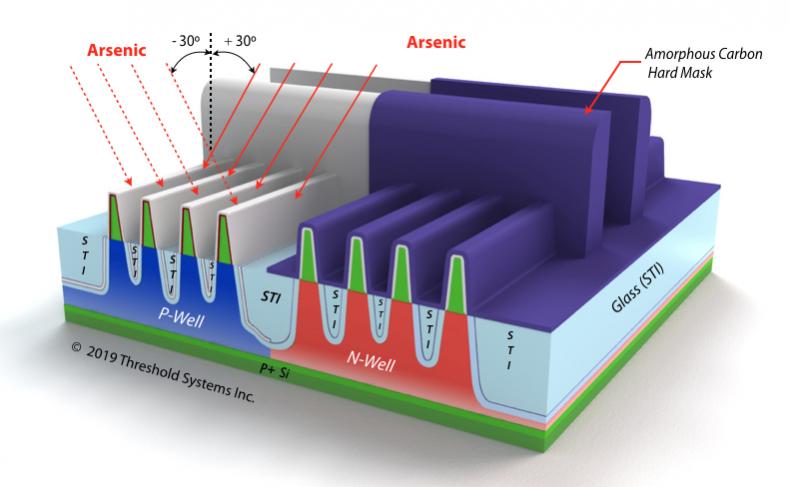
The problem of traditional FinFET Extension Implant doping concerns the awkward 3-dimensional structure of the fin. Because the Extension Implant defines the conductive electrical pathway between the Source/Drains and the undoped channel portion of the fin, it is essential that the fin be uniformly doped all three of its surfaces (the two sides and the top of the fin). The use of a short Amorphous Carbon implant mask helps enormously with this implant because is enables a steep +/- 30º implant angle that allows more of the dopant to be retained on the fin as discussed in part one of this series (refer to figure #1).


Figure #1

Implanting the fin with such a steep double implant allows each side of the fin to be adequately doped, but has the disadvantage that the top of the fin experiences both of these implants (refer to figure #2). This means that the top of the fin is doubly doped and becomes the most conductive fin element. This results in non-uniform fin conductivity that adversely affects transistor performance.


Figure #2

An alternative doping methodology that results in uniform doping on all three sides of the fin is required. This task can be accomplished with two additional masking and implant steps, a nitride deposition and etch operation, followed by a selective oxidation.

The process begins with a masking operation that covers up the N-Wells and exposes the NMOS devices located n the P-Wells. This is followed by an Arsenic implant at 90 degrees into the NMOS fins. (refer to figure #A). This will dope the top of the NMOS fins. However, because the fins are very vertical at the 14/10nm nodes, very little if any dopant will be implanted into the fin sidewalls.

Next, the photoresist is stripped and new photoresist is patterned that covers the P-wells and exposes the N-Wells where the PMOS transistors are located. A 90 degree Boron implant followed by a Carbon locking implant dopes only the top of the PMOS fins (refer to figure B).

Next, a thin nitride layer is blanket deposited across the wafer using Atomic Layer Deposition (refer to figure C). The nitride layer is then etched in a highly anisotropic etch that forms nitride spacers on the gate electrodes and the fins. This is followed by a mild oxide etch that removes the thin layer of oxide on top of the gate electrodes and the top of the fins and exposes the underlying silicon in these areas (refer to figure D).

The wafers then undergo an oxidation step. The Nitride acts as an oxygen barrier and prevents oxide from growing on the surfaces that it covers. However, on the exposed surfaces (the top of the fins and the top of the Gate Electrode) a thick layer of oxide grows (refer to figure E). This thick layer of oxide will act as an implant mask in the following Extension implant operations.

The nitride layer is then stripped from the wafer (refer to figure F). This step is followed by the deposition and patterning of a hard mask that after patterning will cover the N-Well and expose the NMOS devices in the P-Well.

The Extension implants for the NMOS devices are then conducted as illustrated in Figure #3.


Figure #3

However, since the top of the fins are now covered in a thick oxide, only the sidewalls of the fins will experience the +/- 30 degree double implant. This is because although the dose of the Extension implant is very high (10[SUP]15[/SUP] ion/cm[SUP]2[/SUP]), the energy of this implant is very low. The dopant from this implant will be able to penetrate the thin oxide along the sidewalls of the fin, but not the thicker oxide at the top of the fin (refer to figure #4).


Figure #4

The Extension implant is then repeated for the PMOS fins using Boron and Carbon.

This methodology ensures that the fins experience a uniform Extension implant across the top and on both sides of the fin and avoids the double implant of the fins on their upper surfaces that is common in more conventional implant schemes. However, such uniform fin doping is accomplished at the expense of significantly greater processing.

For more information on this topic and for detailed information on the entire process flows for the 10/7/5nm nodes attend the course “Advanced CMOS Technology 2019” to be held on May 22, 23, 24 in Milpitas California.

Also read: The Evolution of the Extension Implant Part 2


Tesla: The Day the Industry Stood Still

Tesla: The Day the Industry Stood Still
by Roger C. Lanctot on 05-05-2019 at 7:00 am

Tesla Motors held an investor event at its Palo Alto headquarters. CEO Elon Musk and a series of Tesla executives announced a new in-house developed microprocessor (already in production and being deployed in Tesla vehicles) and its plans and progress toward autonomous vehicle operation.

Tesla Autonomy Day Live Stream

To be clear – all Tesla vehicles are now getting the new processor the performance of which will be defined by software delivered via over-the-air updates. It’s a minor point for Tesla, which has been doing software updates for years. It’s a monumental change in business practices for the industry.

Musk and his colleagues held forth from a stage in front of an audience of rapt analysts and investors whose silence reflected the collective inhale being experienced across the entire automotive industry and supply chain. Musk’s announcement marked yet another key turning point for the company. He said Tesla is now focused completely on enabling automated driving with the objective of launching a fleet of robotaxis by the end of 2020.

The new microprocessor was the focal point of the event. Musk and his lead designer noted multiple performance advantages over the existing Nvidia hardware in use in older Tesla vehicles. (Nvidia released a blog today challenging and correcting some of Tesla’s claims.)

The event was preceded by Easter weekend news of a Tesla Model S bursting into flames in a parking garage in China and rumors of declining vehicle shipments in advance of Wednesday’s earnings report. Unfazed, Musk took the occasion to cast some shade on erstwhile supplier Nvidia while pointing out what he described as “the fool’s errand” of trying to use lidar technology to enable automated driving.

Despite the fact that so many organizations large and small are working on self-driving car technology, Musk has emerged from the autonomous driving mosh pit as a thought leader matched only in media-attention-getting magnitude by Amnon Shashua of Mobileye. Interestingly, both Shashua and Musk share the same vision of camera-centric automated driving enhanced with ultrasonic and forward facing radar sensors.

There are other contenders for the thought leadership throne in automated driving including Kyle Vogt at Cruise Automation, Jensen Huang of Nvidia, Gil Pratt at Toyota Research Institute, George Hotz formerly of Comm.ai, and Sebastian Thrun and Anthony Levandowski formerly of Google. But only Musk can stop the automotive industry in its tracks with his pronouncements regarding the future of autonomy commanding, as he does, a fleet of hundreds of thousands of connected vehicles.

Musk is the ultimate disruptor – if not outright shredder – of the automotive industry. His investments in electrification are an existential threat to 50% of the industry’s existing internal combustion-centric supply chain.

A Tesla’s engine is its microprocessor and Musk made clear his intention to use that engine in combination with crowd sourced data to refine the software necessary to go with the new chip to enable automated driving. Musk’s core message from the event was that the new chip is capable of enabling full automation, once the software is refined and deployed.

The key takeaways from yesterday’s event included:

  • Lidar is a dead-end, waste of time for autonomous vehicle development
  • High definition maps are unnecessary to enabling automated driving
  • The software code in the new processors are cryptographically signed meaning they can only run Tesla-approved/signed code
  • The new processors are already being built into Model S, X, Y, and 3 vehicles
  • Work on the next generation processor is already well under way, a couple years from completion and will offer a 3X performance gain

Post-event, a bruised Nvidia was quick to note in a blog that its own AI computing hardware offers competitive performance and is “available for the industry to build on” – unlike Tesla’s.

Musk’s pronouncements detonate in the midst of an autonomous vehicle development environment coming to grips with deferred expectations. The growing recognition of the enormity of the technical challenge appears to have caused many market participants to reconsider their public comments or their inclination to say anything at all about their methodology or strategy.

In this environment, Musk’s voice remains loud, clear and unwavering – and automotive executives know they can’t afford not to listen. We may not know for quite some time whether Musk is right on all points. But alone, among many contenders, he is outspoken about his own strategy and opinionated regarding paths – or the path – to autonomy.
Musk, like his competitors, is facing a major leap of faith and technical achievement to deliver fully automated driving. But he must face the fact that lives have been lost in his pursuit of autonomy and skeptics remain.
Only one thing is clear. Musk stands alone in the global industry with the greatest trove of automated and non-automated driving data. At the event he even went so far as to question the efficacy of using simulation software as an alternative to the data collected from human driven miles.

So Musk would and will do without lidar, high definition maps, nvidia, and simulation in his autonomous quest. It remains to be seen how tolerant consumers, investors and regulators will remain should fatalities or flaming cars continue to manifest. Musk remains focused and affirmative – unfortunately he is also fallible. We can only hope no more lives will be lost to Musk’s margin of error.


TSMC and Samsung 5nm Comparison

TSMC and Samsung 5nm Comparison
by Scotten Jones on 05-03-2019 at 7:00 am

Samsung and TSMC have both made recent disclosures about their 5nm process and I though it would be a good time to look at what we know about them and compare the two processes.

A lot of what has been announced about 5nm is in comparison to 7nm so we will first review 7nm.

7nm
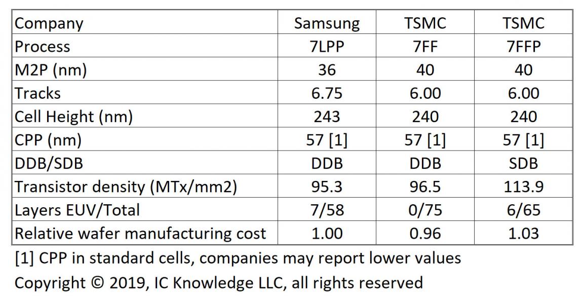
Figure 1 compares Samsung’s 7LPP process to TSMC’s 7FF and 7FFP processes. The rows in the table are:

  • Company name
  • Process name
  • M2P – metal 2 pitch, this is chosen because M2P is used to determine cell height
  • Tracks – the number of metal two pitches in the cell height
  • Cell height – the M2P x Tracks
  • CPP – contacted polysilicon pitch
  • DDB/SDB – double diffusion break (DDB) or single diffusion break (SDB). DDB requires an extra CPP in width at the edge of a standard cell
  • Transistor density – this is uses the method popularized by Intel that I have written before where two input NAND cell size and scanned flip flop cell sizes are weighted to give a transistors per millimeter metric
  • Layers – this is the number of EUV layers over the total number of layers for the process
  • Relative cost – using Samsung’s 7LPP cost as the baseline we compare the normalized cost of each process to 7PP. The cost values were calculated using the IC Knowledge – Strategic Cost Model – 2019 – revision 01 versions for a new 40,000 wafers per month wafer fabs in either South Korea for Samsung or Taiwan for TSMC
    Figure 1. 7nm comparison


    Looking at figure 1 it is interesting to note that Samsung’s 7LPP process is less dense than either of TSMC’s processes in spite of using EUV and having the smallest M2P. TSMC more than makes up for Samsung’s tighter pitch with a smaller track height and then for 7FFP a SDB. For TSMC 7FF without EUV moving to 7FFP with EUV reduces the mask count and adds SDB improving the density by 18%.

    Now that we have a solid view of 7nm we are ready to look forward to 5nm:

    5nm
    Both Samsung and TSMC have started taking orders for 5nm with risk production this year and high-volume production next year. We expect both companies to employ more EUV layers at 5nm with 12 for Samsung and 14 for TSMC.

    Samsung has said their 5nm process offers a 25% density improvement over 7nm with a 10% performance boost or 20% lower power consumption. My understanding is the difference between 7LPP and 5LPE for Samsung is a 6-track cell height and SDB. This results in a 1.33x density improvement.

    This contrasts with TSMC who announced a 1.8x density improvement and a 15% performance improvement or 30% lower power. I recently saw another analyst claim that Samsung and TSMC would have similar density at 5nm, that one really left me scratching my head given that the two companies have similar 7nm density and TSMC has announced a much larger density improvement than Samsung. My belief is that TSMC will have a significant density advantage over Samsung at 5nm.

    Figure 2 summarizes the two processes using the same metrics as figure 1 with the addition of a density improvement versus 5nm row.

    Figure 2. 5nm comparison


    From figure 2 you can see that we expect TSMC to have a 1.37x density advantage over Samsung with a lower wafer cost!

    Another interesting item in this table is TSMC reaching 30nm for M2P. We have heard they are being aggressive on M2P with numbers as low as 28nm mentioned. We assumed 30nm as a slight relaxation from the 28nm number to produce the 1.8x density improvement, TSMC had at one time said 5nm would have a 1.9x density improvement.

    Conclusion
    We believe TSMC’s 5nm process will significantly outperform Samsung’s 5nm process in all key metrics and represent the highest density logic process in the world when it ramps into production next year.

    For more information on TSMC’s leading edge logic processes I recommend Tom Dillinger’s excellent summary of TSMC’s technology forum available here.


Webinar: ISO 26262 Compliance

Webinar: ISO 26262 Compliance
by Daniel Payne on 05-02-2019 at 12:00 pm

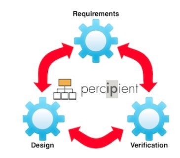
To me the major idea of ISO 26262 compliance is ensuring that requirements can be traced throughout the entire design and verification process, including the use of IP blocks. The first market application that comes to mind with ISO 26262 is automotive, with its emphasis on safety because human lives are at stake. Since necessity is the mother of all invention, we have software vendors that have focused on automating this big challenge of traceability of requirements, design data and verification results. Methodics is a software vendor focused on this area, and they are organizing a webinar:

  • Achieving a Traceable Semiconductor Design and IP Methodology for ISO 26262 Compliance
  • Tuesday, May 14, 2019 at 10AM Pacific Time
  • Registration Online

Percipient is the IP Lifecycle management tool discussed in the webinar, and it provides a fully traceable environment for tracking IP in a company while engineers go about their design and verification tasks: analog, digital, software, embedded software, final assembly. The beauty of using Percipient is that traceability is already built-in to the process.

Speakers

Michael Munsey
VP Business Development and Strategic Accounts
Methodics Inc.

Michael Munsey has over 25 years experience in Engineering Design Automation and Semiconductor Companies. Prior to joining Methodics, Michael was Senior Director of Strategy and Product Marketing for semiconductors, software life cycle management, and IoT at Dassault Systemes. Along with strategic initiatives, he was responsible for business development, partnerships, and cross-industry initiatives such as automotive electronics, and M&A in the above areas. Michael began his career with IBM as an ASIC designer before making the move over to EDA where he has held various senior and executive-level positions in marketing, sales, and business development. He was a member of the founding teams for Sente and Silicon Dimensions, and also worked for established companies including Cadence, VIEWLogic, and Tanner EDA. Michael received his BSEE from Tufts University.


Rien Gahlsdorf
Director of Application Engineering
Methodics Inc.

Rien Gahlsdorf is the Director of Application Engineering at Methodics where he endeavors to create a clear customer understanding of the product, and a clear product alignment with the customer. Rien brings over 20 years of experience in product development and support, technical sales, and analog and RF design to his role at Methodics, which he joined in 2016. Rien received his MBA from Boston University.


Vishal Moondhra
VP of Solutions Engineering
Methodics Inc.

Vishal Moondhra has over 20 years experience in Digital Design and Verification. He has held engineering and senior management positions with innovative startups including IgT and Montalvo, and large multinationals including Intel and Sun. In 2008, Vishal co-founded Missing Link Tools, which built the industry’s first comprehensive DV management solution, bringing together all aspects of verification management. Methodics acquired Missing Link Tools in 2012.