Safety, especially in road vehicles (cars, trucks, motorcycles, etc.), gets a lot of press these days. From the point of view of vendors near the bottom of the value chain it can seem that this just adds another item to the list of product requirements; as long as you have that covered, everything else remains pretty much the same in your business cycle. That would be nice but it’s quite inaccurate at least for those selling components, such as IP, which wind up in the final product.
Back in the mists of time (5 years or so ago), vehicle electronics were pretty simple: a number of small control units, simple 16-bit or maybe 32-bit MCUs, spread around the car to handle braking, engine control chassis control and so on. Then we all got excited about putting more intelligence into our ride. Automakers started with automated driving assistance – lane keeping, intelligent cruise control and the like. This takes real compute horsepower, far beyond the capabilities of an MCU. And decisions you want these engines to make, such as, “should I brake because I see a pedestrian crossing the road”, can’t be distributed around the car. So the next logical step was to architect for a central brain, digesting sensor input from around the car in support of its decisions.
Which in part drove the need for Automotive Ethernet, because that’s a lot of data you have to send – just think of a video stream from a camera. And we realized we needed a lot of these sensors, partly to cover different directions but also for different capabilities – more cameras, radar and lidar for ranging and speed information for objects around the car and ultrasonic sensors for parking control. Each pumping masses of data to that central brain to drive time-critical decisions.
Hmm – maybe need to rethink the architecture a bit. So we are now adding more intelligence to the sensors, increasingly in ASICs for performance, so they can just send back object lists rather than raw images to reduce the load on the Ethernet. But that’s not quite right either because sometimes we want both objects and images – detect a pedestrian but also show the image on the cabin monitor so the driver can decide if she thinks there’s really a problem or not. Then there’s sensor fusion; maybe recognition needs to look at both the camera and radar images, not just objects, to draw a conclusion. Bottom-line, there is no “right” architecture – central or distributed or a mix – at least today, so OEMs pick candidates which best serve their competitive and safety needs. Here, Safety of the Intended Function (SOTIF, beyond 26262) is also becoming more prominent although it’s unclear yet how this will affect hardware developers; it would be surprising to hear it will have no impact.
Then you get down to building these chips for which you have to ensure functional safety. Systematic errors are dealt with through the process side of ISO 26262 on which I and others have already written plenty. Random errors triggered by cosmic ray-induced ionization are also a concern. Back in those same mists of time, processes use for automotive electronics were, per Kurt Shuler (VP marketing at Arteris IP) “Cro-Magnon”; 50nm or thereabouts, less susceptible to this kind of problem. But you can’t build these big ML-centric chips in 50nm; ADAS devices are now going into 7nm where ionization is much more of a problem. In your phone or TV, this is not a big deal, but in a safety-critical system random errors have to be weeded out, at minimum by detection, better still by correction. In ISO 26262 Part 2, you and the integrator need to deliver credible evidence that the safety mechanisms provided are sufficient.
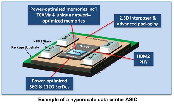
Since I’m talking about Arteris IP, the interconnect between CPUs and ML accelerators and all the other goodies in these big devices, this runs to tens of millions of gates itself, a major candidate for random error detection/correction. This can be through parity checks, ECC or even logic duplication with units running in lockstep. Though of course where to insert such mechanisms rests on decisions the integrator will make based on failure mode effects and diagnostic analysis (FMEDA) with planned detection/mitigation fixes. A network-on-chip (NoC) interconnect is built bottom-up so the safety mechanisms can be programmed in, as needed, bottom-up. Other IPs will often have to work harder to provide similar levels of protection (and confidence); retro-fitting safety is a lot harder than designing it in from the outset.
So far, so complicated, though maybe no big surprises above what you already knew. But now look at the support and business cycle from an IP vendor point of view. During design, the vendor supports the integrator in joint discussions on how to meet functional safety goals with respect to that IP and helping the architect and integrator as needed. The integrator tapes out, when everything goes relatively quiet for maybe a year or more as the integrator works with their customer, maybe a tier 1. Then requests start rolling back to you; the integrator wants to know more about how something was designed, for verification reports and confirmation measures and you have to support them in their responses. Point being that “signoff”, measured by when you get paid, moves higher in the chain and later. Kurt said they have seen 5-6 years in one case, although competitive pressures are driving that down somewhat. Royalties as always come later still. Another twist; IP vendors now have to keep everything that was built in a lock box for 10 years.
Still think you want to sell IP into the automotive chain? There’s certainly a lot of promise. More big chips in the central brain and in intelligent sensors together offer a lot of opportunity. The US, Europe and Israel markets are all very aggressive in developing ADAS and ML. China has been a laggard but is coming on strong and is not held back by legacy so much. They also see a big tie-in with AI where they are very strong. Kurt tells me there are over a couple of hundred funded startups in automotive and AI in China.
That said, this is not an easy way to get rich. You’ll have to put a lot of investment into supporting your customers, supporting their customers and so on up to the top. The market is very dynamic, so what “done” means may not always be clear. You may not be paid for quite a long time. But if you have the grit to hang on and keep your customer happy the whole way through, you might just be successful!