Our friends at Threshold Systems have a new ONLINE class that may be of interest to you. It’s an updated version of the Advanced CMOS Technology class held last February. This is normally a classroom affair but to accommodate the recent COVID-19 travel restrictions it is being offered virtually.
As part of the previous class we did a five part series on The Evolution of the Extension Implant which you can see on the Threshold Systems SemiWiki landing page HERE. Registration is HERE. And here is the updated course description:
Course Description:
The central theme of this seminar is an in-depth presentation of the key 10/7/5 nm node technical issues for Logic and Memory, including detailed process flows for these technologies.
This course addresses the issues associated with Advanced CMOS manufacturing with technical depth and conceptual clarity, and presents leading-edge process solutions to the new and novel set of problems presented by 10nm and 7 nm FinFET technology and previews the upcoming manufacturing issues of the 5 nm Nanowire.
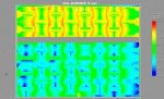
A key part of the course is a visual survey of leading-edge devices in Logic and Memory presented by the Fellow Emeritus of the world’s leading reverse engineering firm, TechInsights. His lecture is a visual feast of TEMs and SEMs of all of the latest and greatest devices being manufactured and is one of the highlights of the course.
An update on the status of EUV lithography will be also be presented by a world-class lithographer who manages an EUV tool. His explanations of how this technology works, and the latest EUV breakthroughs, are enlightening as they are insightful.
Finally, a detailed technology roadmap for the future of Logic, SOI, Flash Memory and DRAM process integration, as well as 3D packaging and 3D Monolithic fabrication will also be discussed.
Each section of the course will present the relevant technical issues in a clear and comprehensible fashion as well as discuss the proposed range of solutions and equipment requirements necessary to resolve each issue.
Course Notes:
The course notes are technically current, reproduced in high-resolution color and profusely illustrated with 700+ pages of high-quality 3D graphics and TEMs of real-world devices.
In addition, dynamic 3D models of semiconductor micro-structures are presented on-screen to clarify the structural details of FinFETs, 3D Flash and Nanowires. Click on the link below to preview a typical dynamic 3D image.
| Date: |
May 27, 28, 29, 2020 |
| Location: |
This course is held ONLINE |
Class Schedule:
|
Wednesday: 8:30 AM – 5:00 PM, PDT
Thursday: 9:00 AM – 5:00 PM, PDT
Friday: 9:00 AM – 5:00 PM, PDT |
| Tuition: |
$1,695 |
Online Instruction:
The Covid-19 pandemic and the travel restrictions it has imposed have changed the landscape of technical instruction from traditional instructor-lead classroom learning and toward a distributed learning experience that enables the instructor and the students to be in different locations. This learning solution eliminates high cost and inconvenience associated with having students travel to one location for instruction. It offers a flexibility and a convenience that traditional classroom instruction does not have. It is ideal for companies with a global business model and whose employees are scattered around the world.
The benefits of Online Learning are numerous:
- a safe environment for both the students and the instructor
- elimination of instructor travel costs
- elimination of employee travel and lodging costs
- minimal disruption of employee work schedules
- reduced enrollment costs
- the students do not all have to be in a single location. Remote Learning permits student attendance even if they are located in different countries.
- unlike watching streamed video, remote instruction closely simulates the classroom experience and permits student questions and real-time student/instructor interaction
How Online Learning Works:
Shortly after you register a link will be emailed to you that will take you to the online classroom the day of the course, and the week before the class begins a binder of color course notes will be shipped to you via Fedex or UPS.
The class is three days long and will begin on May 27, 2020 at 8:30 PDT. On that day you simply click on the link that has been provided and you will be seamlessly taken to the online classroom. There you will see the opening slide of the course and a small inset image of the instructor. Once the class begins you will hear the instructors voice as he addresses the technical issues on each slide being presented. There will be a one-to-one correspondence between the slides being presented on the screen and the slides in your binder of course notes. Questions can be asked at any time by typing in the software’s question box and each question will be answered verbally by the instructor as soon as they are received.
In the unlikely event that you experience technical difficulties an IT expert will be on-hand to resolve any issues for you in real time.
Online learning is a simple, safe and convenient way to learn that offers a highly effective classroom experience without having to leave the safety and comfort of your own home or office.
What’s Included:
- Three days of instruction by industry experts with comprehensive, in-depth knowledge of the subject material
- A high quality set of full-color lecture notes, including SEM & TEM micrographs of real-world IC structures that illustrate key technical points
- A Diploma stating that you have successfully completed the seminar will be mailed to you at the end of the course
Who is the seminar intended for:
- Equipment Suppliers & Metrology Engineers
- Fabless Design Engineers and Managers
- Foundry Interface Engineers and Managers
- Device and Process Engineers
- Design Engineers
- Product Engineers
- Process Development & Process Integration Engineers
- Process Equipment Marketing Managers
- Materials Supplier Marketing Managers & Applications Engineers
Course Topics:
1. Process integration
The 10/7nm technology nodes represent a landmark in semiconductor manufacturing and they employs transistors that are faster and smaller than anything previously fabricated. However, such performance comes at a significant increase in processing complexity and requires the solution of some very fundamental scaling and fabrication issues, as well as the introduction of radical, new approaches to semiconductor manufacturing. This section of the course highlights the key changes introduced at the 10/7nm nodes and describes the technical issues that had to be resolved in order to make these nodes a reality.
- The enduring myth of a technology node
- Market forces: the shift to mobile
- The Idsat equation
- The motivations for High-k/Metal gates, strained Silicon
- Sevice scaling metrics
- Ion/Ioff curves, scaling methodology
2. Detailed 10nm Fabrication Sequence
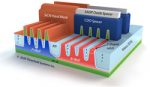
The FinFET represents a radical departure in transistor architecture. It also presents dramatic performance increases as well as novel fabrication issues. The 10nm FinFET is the 3rd generation of non-planar transistor and involves some radical changes in manufacturing methodology. The FinFET’s unusual structure makes its architecture difficult for even experienced processing engineers to understand. This section of the course drills down into the details of 10nm FinFet structure and its fabrication, highlighting the novel manufacturing issues this new type of transistor presents. A detailed step-by-step 10nm fabrication sequence is presented (Front-end and Backend) that employs colorful 3D graphics to clearly and effectively communicate the novel FinFET architecture at each step of the fabrication process. Attention to key manufacturing pitfalls and specialty material requirements are pointed out at each phase of the manufacturing process, as well as the chemistries used.
- Self-Aligned Quadruple Patterning (SAQP)
- Fin-first and Fin-last integration strategies
- Multiple Vt Hi-/Metal Gate integration strategies
- Cobalt Contacts & Cobalt metallization
- Contact over Active Gate methodology
- Advanced Metallization strategies
- Air-gap dielectrics
3. Nanowire Fabrication – the 5nm Node
Waiting in the wings is the Nanowire. The advent of this new and radically different 3D transistor features gate-all-around control of short channel effects and a high level of scalability. A detailed process flow of a Horizontal Nanowire fabrication process will be presented that is beautifully illustrated with colorful 3D graphics and which is technically accurate.
- A step-by-step Horizontal Nanowire fabrication process flow
- Key fabrication details and manufacturing problems
- Nanowire SCE control and scaling
- Resolving Nanowire capacitive coupling issues
- Vertical versus Horizontal Nanowire architecture: advantages and disadvantages
4. DRAM Memory
DRAM memory haS evolved through many generations and multiple incarnations. Despite claims that DRAM memory is nearing its scaling limit, new technological developments keep pushing the scaling envelope to extremes. This part of the course examines the evolution of DRAM memory and presents a detailed DRAM process fabrication flow.
- DRAM memory function and nomenclature
- DRAM scaling limits
- A DRAM process flow
- The capacitor-less DRAM memory cell
5. 3D NAND Flash Memory
The advent of 3D NAND Flash memory is a game changer. 3D NAND Flash not only dramatically increases non-volatile memory capacity, it will also add at least three generations to the life of this memory technology. However, the structure and fabrication of this type of memory is radically different, even alien, to any traditional semiconductor fabrication methodology. This section of the course presents a step-by-step visual description of the unusual manufacturing methodology used to create 3D Flash memory, focusing on key problem areas and equipment opportunities. The fabrication methodology is presented as a series of short videos that clearly demonstrate the fabrication operations at each step of the process flow.
- staircase fabrication methodology
- the role of ALD in 3D Flash fabrication
- controlling CDs in tall, vertical structures
- detailed sequential video presentation of Samsung 3D NAND Flash
- Intel-Micron 3D NAND Flash fabrication sequence
- Toshiba BICS NAND Flash fabrication sequence
6. Advanced Lithography
Lithography is the “heartbeat” of semiconductor manufacturing and is also the single most expensive operation in any fabrication process. Without further advances in lithography continued scaling would difficult, if not impossible. Recently there have been significant breakthroughs in Extreme Ultra Violet (EUV) lithography that promise to radically alter and greatly simplify the way chips are manufactured. This section of the course begins with a concise and technically correct introduction to the subject and then provides in-depth insights into the latest developments in photolithography. Special attention is paid to EUV lithography, its capability, characteristics and the recent developments in this field.
- Physical Limits of Lithography Tools
- Immersion Lithography – principles and practice
- Double, Triple and Quadruple patterning
- EUV Lithography: status, problems and solutions
- Resolution Enhancement Technologies
- Photoresist: chemically amplified resist issues
7. Emerging Memory Technologies
here are at least three novel memory technologies waiting in the wings. Unlike traditional memory technologies that depend on electronic charge to store data, these memory technologies rely on resistance changes. Each type of memory has its own respective advantages and disadvantages and each one has the potential to play an important role in the evolution of electronic memory.
This section of the course will examine each type memory, discuss how it works, and what its relative advantages are in comparison with other new memory types.
- Phase Change Memory (PCRAM), Cross-point memory; separating the hype from the reality
- Resistive RAM (ReRAM) – a novel approach that comes in two variations
- Spin Torque Transfer RAM (STT-RAM) – the brightest prospect?
8. Survey of leading edge devices
This part of the course presents a visual feast of TEMs and SEMs of real-world, leading edge devices for Logic, DRAM and Flash memory. The key architectural characteristics for a wide range of key devices will be presented and the engineering trade-offs and compromises that resulted in their specific architectures will be discussed. The Fellow Emeritus representative of the world’s leading chip reverse engineering firm will present the section of the course.
- How to interpret Scanning and Transmission Electron microscopy images
- A visual evolution of replacement gate metallization
- DRAM structural analysis
- 3D FLASH structural analysis
- Currently available 14nm/10nm/7nm Logic offerings from various manufacturers
9. 3D Packaging Versus 3D Monolithic Fabrication
Unlike all other forms of advanced packaging that communicate by routing signals off the chip, 3D packaging permits multiple chips to be stacked on top of each other, and to communicate with each other using Thru-Silicon Vias (TSVs), as if they were all one unified microchip. An alternate is the 3D Monolithic approach, in which a second device layer is fabricated on a pre-existing device layer and electrically connected together employing standard nano-dimensional interconnects. Both approaches have advantages and disadvantages and promise to create a revolution in the functionality, performance and the design of electronic systems.
This part of the course identifies the underlying technological forces that have driven the development of Monolithic fabrication and 3D packaging, how they are designed and manufactured, and what the key technical hurdles are to the widespread adoption of these revolutionary technologies.
- TSV technology: design, processing and production
- Interposers: the shortcut to 3D packaging
- The 3D Monolithic fabrication process
- Annealing 3D Monolithic structures
- The Internet of Things (IoT)
10. The Way forward: a CMOS technology forecast
Ultimately, all good things must come to an end, and the end of FinFET technology appears to be within sight. No discussion of advanced CMOS technology is complete without a peek into the future, and this final section of the course looks ahead to the 5/3.5/2.5 nm CMOS nodes and forecasts the evolution of CMOS device technology for Logic, DRAM and Flash memory.
- Is Moore’s law finally coming to an end?
- New nanoscale effects and their impact on CMOS device architecture and materials
- The transition to 3D devices
- Future devices: Quantum well devices, Nanowires, Tunnel FETs, Quantum Wires
- The next ten years …
REGISTER NOW!


