You are currently viewing SemiWiki as a guest which gives you limited access to the site. To view blog comments and experience other SemiWiki features you must be a registered member. Registration is fast, simple, and absolutely free so please, join our community today!
This is a live panel with industry experts who are on the leading edge of AI in semiconductor manufacturing. This is a must attend event for all levels of semiconductor professionals. I hope to see you there.
The semiconductor industry faces unprecedented challenges as it pushes toward advanced nodes below 3nm, managing exponential process complexity, yield variability, and escalating production costs.
This webinar explores the transition from reactive automation to autonomous manufacturing, bringing together leaders from across the semiconductor ecosystem. Experts will examine how AI-driven digital twins, predictive metrology, agentic AI systems, and generative design are revolutionizing yield management and sustainability.
Discover how cross-ecosystem collaboration and intelligent fab assistants are overcoming the limitations of traditional manufacturing models. From inline defect classification to AI copilots for process engineers, these innovations are paving the way for self-optimizing ‘AI Factories’ that will define the future of global microelectronics as conventional approaches to reach their limits.
Date: April 23rd, 2026 Time: 10:00 AM PDT Duration: 60 minutes
Agenda
(5min) Introductions- Daniel Nenni, SemiWiki
(10 min) Dr. Janhavi Giri, EDA & Semiconductor Industry Vertical Lead, NetApp
Presentation on “Beyond Moore’s Law: The Future of Semiconductor Manufacturing Intelligence”
Panel session (45-min)
Dr. Jim Shiely, Director, R&D Calibre Semi Manufacturing, Siemens EDA
Dr. Larry Melvin, Sr. Director, Technical Product Management, Synopsys
Dr. Christophe Begue, VP, Corporate Strategic Marketing, PDF Solutions
Dr. Janhavi Giri, EDA & Semiconductor Industry Vertical Lead, NetApp
Daniel Nenni, SemiWiki Founder (Moderator)
Who Should Attend
Semiconductor fab, manufacturing, and yield leaders
Process and device engineers at advanced nodes
AI, data, and automation teams driving smart factories
Digital transformation and technology executives
Equipment, EDA, and ecosystem partners
Key Takeaways
How AI is enabling autonomous, self optimizing semiconductor manufacturing
Practical use of digital twins, predictive metrology, and agentic AI
New approaches to yield improvement, cost reduction, and sustainability
The role of intelligent fab assistants and cross ecosystem collaboration
Review the specifications of any state-of-the-art microcontroller and you will discover the high dynamic current the device can consume. Examining the high clock rates and low tolerable voltage drop will lead you to the all-important power delivery network, or PDN. Components here include power planes, layer stack-up, decoupling capacitors, and a voltage regulator module. The quality of the PDN can have a big impact on overall product performance. The goal is to deliver a stable supply voltage with low voltage drop across the entire specified temperature range throughout the product’s lifetime.
Getting all this right can be quite daunting. Siemens recently released a white paper on this topic. Predominant failure mechanisms for PDN designs are discussed, along with how to avoid them. There is a lot of great information here. A link is coming so you can get the whole story but first let’s see what exploring the hidden complexity of modern power electronics design reveals in this Siemens white paper.
What’s at Stake
An improperly designed PDN can create many issues, some immediate and others are like a ticking time bomb. An example is high voltage drop due to narrow traces. In this case, the result is reduced timing margin that can cause products to fail. This effect may not manifest at room temperature but rather at higher temperatures or after years of field operation. The impact of such field failures is unforeseeable but can be avoided by applying the capabilities of integrated simulation tools.
It’s important to note that the interaction between electrical, thermal, and reliability constraints is far more complex than most traditional workflows can typically capture. In addition, it’s crucial to understand PDN modelling to ensure efficiency during the design process and to guarantee deterministic behavior across all load states and switching events.
The white paper goes on to point out that the journey from a perfect schematic to field failures is not intuitive, but the significant amount of design constraints increases the complexity for modern power electronics. For example, even a simple current-mode pulse-width-modulated controller, such as the LM5020 has about 40 explicit design constraints for using the part. Not handling those constraints across the electrical, thermal, mechanical, and manufacturing domains, along with the associated complexity, can lead to field failures.
With this backdrop, the white paper discusses the four predominant PDN failure mechanisms to illustrate the necessity of a highly integrated design and verification flow. The graphic at the top of this post summarizes those four failure mechanisms.
What to Focus On
Here is a short summary of the PDN failure mechanisms discussed in the white paper.
1) Improper stackup: Printed circuit board (PCB) failures often originate from insufficient control of the PDN, whose impedance must remain low across a wide frequency range to ensure stable IC supply conditions. The white paper explains that PDN behavior is strongly influenced by layer stackup configuration, dielectric spacing, power-plane geometry, and decoupling-capacitor placement.
Improper choices in these areas leads to increased impedance, resonant peaks, and voltage ripple, all of which reduce design margin and increase susceptibility to field failures.
2) Capacitor selection: While layer stack-up and power-plane spacing define the baseline impedance profile of the PDN, the white paper points out that impedance is not static over the system lifetime. In addition to geometry-induced resonances, time- and temperature-dependent degradation of decoupling capacitors progressively alters the PDN characteristics and dominates long-term reliability and failure behavior.
3) Thermal and environmental stress: Beyond purely electrical phenomena such as PDN resonances and decoupling degradation, the white paper also points out that long-term system reliability is governed by a broader set of interacting effects. Here, mechanical, thermal, and environmental stressors couple with electrical loading and material properties, giving rise to cumulative damage mechanisms that cannot be captured by electrical analysis alone.
The white paper presents a physics of failure (PoF)-based methodology for predicting the lifetime of power electronics at the PCB level during early design stages. There are a lot of details covered in this approach. A summary of the methodology is shown below to give you an idea of what’s involved.
Application of physics of failure for power electronics
4) Using components out of the specification: After addressing electrical, mechanical, and aging-related failure mechanisms at the system level, the white paper revisits failures that originate directly from component operating conditions. It is pointed out that operation beyond specified electrical and thermal limits remains a dominant root cause of semiconductor failures and directly constrains PDN design and verification. The dominant failure mechanisms for this class of issues are discussed, along with approaches to address them.
To Learn More
A concluding comment from the white paper is that power electronics has moved beyond simple schematic-driven design. The complexity of modern systems demands automated, multi-domain, simulation-driven workflows that drastically reduce manual effort and improve reliability.
This white paper provides an excellent overview of the key issues designers will face and practical guidance on approaches to address these issues. If you are faced with PDN design challenges this is a must-read white paper. You can get your copy here. And that is what’s involved in exploring the hidden complexity of modern power electronics design.
Daniel is joined by Michael Adeniya, Group Director, Microelectronics Global and a key architect behind the launch of Microelectronics US. Mike is focused on uniting the “Silicon Hills” ecosystem to address the practical engineering bottlenecks of the post CHIPS Act era. By fostering strategic partnerships with leaders like Silicon Catalyst, RISC-V, Edge AI Foundation and more.
Dan begins the discussion by exploring the motivation and goals behind the work Michael is doing at Microelectronics Global. Michael explains that he is developing industry events that provide impact and focus for collaboration well beyond the event’s few days. The Microelectronics US event is designed to accomplish this goal. Michael explains the event is set in Austin, Texas, an under-served vibrant community that provides an excellent backdrop for the show. The event is free for all to attend, and includes a extensive series of presentations, panels, workshops, executive forums, and social gatherings all focused on collaboration to achieve execution at scale.
The event will cover semiconductors, photonics and embedded systems. Michael explains that many major semiconductor companies will be present at the show along with an array of promising startups. Michael also explains that Silicon Catalyst is a strategic partner for this event and he has already worked with the organization on other successful events. The conference is also offering free exhibit space to qualifying startups.
The event will be held Palmer Events Center in Austin, Texas from April 22-23, 2026. You can learn more about the event and register to attend here.
The views, thoughts, and opinions expressed in these podcasts belong solely to the speaker, and not to the speaker’s employer, organization, committee or any other group or individual.
IoT permeates every aspect of our lives, in payment systems, access authorization, vehicles, utilities, factories, hospitals, and in so many other fields. Which makes these systems attractive targets for hacking and social disruption while also challenging to protect given the highly constrained resources that many such devices can support. Effective defense requires a multi-dimensional post-quantum approach: secure boot, secure TLS (transport layer security) and protection against physical attacks through side-channels. PQShield have announced their MicroCore IP (software only or software plus optional hardware acceleration) to address a wide range of IoT footprints, in as little as 5KB RAM, tuned to the most demanding edge applications.
Secure boot
Post quantum cryptography (PQC) is more expensive than classical cryptography. Keys are bigger and algorithms are bigger, which should be no surprise since the point is to defeat quantum computer (QC) attempts to decode weaker pre-quantum cryptography. Post quantum methods therefore call for very careful design to fit resource constrained edge devices.
“Q-day” (the unannounced date on which QCs will be able to break classical encryption) may arrive within the next 10 years. That’s a problem for products already in place and expected to be in deployment for 10-20 years. Product builders have a range of challenging needs: PQC signature verification to authorize over-the-air boot image updates, deployable as a software-only update with no need to change hardware, compliant with the latest authorized PQC standards: NIST, CNSA, PSA, CAVP, and ISO, and supporting a spectrum of options from low footprint to high speed to ultra secure, also in line with standards.
PQShield claim their MicroLib software IP provides all these capabilities, especially in this context enabling PQC in under 5KB of SRAM. Probably not too surprising since they have been active in this area and with NIST for quite a while.
Transport layer security (TLS)
Edge devices in industrial IoT (IIot) applications depend on secure communication between those devices. The mechanism to ensure this is transport layer security (TLS) which has superseded SSL. TLS is realized through a handshake: client and server agree on a TLS version, the server sends a certificate to prove its identity, then session keys are exchanged to encrypt further communication in that session.
Software-only upgrades requiring minimal memory are especially important here. These so-called “brownfield” upgrades are the only practical option in industries which have established IIoT installations yet are required to become PQC compliant. Ripping out pre-PQC devices and starting again would be wildly impractical, yet the risks and regulatory requirements from the NSA and beyond cannot be ignored.
In support of TLS PQShield offers PQC algorithms, PSA Crypto APIs and MbedTLS, supporting seamless migration to PQC secure without proprietary lock in.
Protection against side-channel attacks (SCA)
Side-channel attacks hack hardware by teasing out crypto information through careful study of timing, power, or logic behavior. This idea really took off in the mid-1990s with a paper published by Kocher. Differential Power Analysis (DPA) is one approach, monitoring power consumption at a very fine level during encryption/decryption and using statistical analysis to progressively infer bits in the key. All methods are non-destructive, but some do need close access to a device to be hacked, not so difficult to accomplish in a large factory.
Methods to defend against SCA include balancing computations during crypto operations so that differences between bits in timing or power (for example) cannot be discerned. Achieving this goal requires additional care in designing PQC algorithms, also careful testing on reference board to ensure that implementations demonstrate very low bit-to-bit variance in these physical parameters. PQShield here also claims thy meet these objectives.
The company recently demonstrated these capabilities at Embedded World. You can learn more HERE and you can contact them at contact@pqshield.com.
In today’s increasingly connected world, there are billions of SoCs, powering everything from automotive ECUs to industrial IoT sensors and processing sensitive data. While software-level security is taken seriously, hardware-level vulnerabilities have often been an afterthought. As hackers are now using more complex tampering techniques, protecting the physical silicon inside devices has become crucial. Analog anti-tamper IP and sensors can play an important role in strengthening hardware security and preventing attacks that lead to unauthorized access or manipulation.
The primary driver for enhanced hardware security is the mass deployment of decentralized connected devices. According to Agile Analog’s agileSecure anti-tamper presentation, more than ten billion IoT devices are currently in the field. These devices are physically accessible to attackers, making them key targets for invasive and non-invasive tampering. At the same time, as organizations transition to AI-heavy workloads, a single hardware breach could compromise the entire Root of Trust (RoT), resulting in catastrophic data loss and costing millions of dollars. As AI models move to silicon, the need for hardened hardware-level security becomes undeniable.
Hardware attacks are increasingly sophisticated. Hackers can manipulate silicon behavior using techniques such as fault injection, glitching and side channel analysis. Fault injection attacks intentionally introduce errors into a system in order to bypass security checks or access confidential information. Similarly, side channel attacks analyze indirect signals such as power supply or execution timing to extract sensitive data such as cryptographic keys. More advanced physical attacks, including micro-probing, laser fault injection and focused ion beam techniques, allow attackers to access internal circuitry directly. Supply chain threats such as hardware trojans, device cloning and reverse engineering create significant risks for both manufacturers and users.
Recent incidents demonstrate how serious hardware vulnerabilities can be. Field data shows several security breaches caused by hardware attacks. In one instance, voltage glitching was used to bypass secure fuses in consumer electronics to dump encrypted firmware. In the automotive sector, infotainment platforms have been compromised through glitching attacks that neutralized digital signature verification. These examples prove that digital-only security is often not sufficient when attackers can physically interact with hardware.
Analog sensors provide an effective way to detect and prevent many of these attacks. Unlike digital sensors, analog anti-tamper sensors monitor the physical operating conditions of the chip itself. They can detect unexpected voltage levels, irregular clock signals, temperature changes or electromagnetic disturbances that may indicate that an attack is taking place. When these abnormal conditions are detected, the system can trigger an immediate hardware-level response, such as zeroizing keys or forcing a reset.
Several different types of analog anti-tamper sensors are used to strengthen hardware security. Voltage glitch detectors monitor the power supply and identify sudden spikes or drops that could be a sign of an attack. Clock attack monitors detect irregular clock behavior such as frequency manipulation or timing glitches. Thermal sensors identify unusual temperature changes that may occur during cold boot attacks designed to extract encryption keys from memory. Electromagnetic sensors detect electromagnetic fault injection attacks that disrupt internal circuits. By combining multiple sensors, engineers can create layered defenses that significantly increase the difficulty of successfully attacking a device.
Despite their importance, designing analog security sensors presents several challenges. Analog circuit design requires specialized expertise and often involves complex and time consuming manual processes. Variations between semiconductor manufacturing technologies can also make it difficult to reuse designs across different process nodes. As companies face shrinking tape-out windows and a shortage of analog design expertise, many may struggle to implement this advanced hardware security.
Agile Analog is helping to address these challenges. Using the company’s unique Composa tool, it is possible to automatically generate analog IP to a customer’s exact specifications, for any foundry and on any process – from legacy nodes to FinFET. Analog security components from the agileSecure anti-tamper security IP portfolio can be developed more efficiently and deployed across multiple semiconductor technologies. This approach reduces development time and cost while maintaining reliability and performance.
Bottom line: Hardware security has become an essential part of modern electronic systems as connected devices and sophisticated attack techniques continue to increase. Analog anti-tamper sensors provide a critical layer of protection by detecting physical attacks that digital security mechanisms cannot prevent. Integrating these analog sensors into semiconductor designs will play a key role in protecting devices, sensitive data and critical infrastructure in the future.
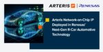
The increasing complexity of advanced driver assistance systems (ADAS) and automated driving architectures has driven a transition from traditional bus-based interconnects to scalable Network-on-Chip (NoC) fabrics. Renesas’ next-generation R-Car automotive SoC platforms adopt Arteris FlexNoC interconnect intellectual property to meet stringent requirements for performance, power efficiency, and functional safety. This deployment represents a critical architectural shift toward heterogeneous computing and software-defined vehicle (SDV) architectures in modern automotive electronics.
Arteris is a leading semiconductor IP provider specializing in NoC interconnect technologies designed to optimize on-chip communication between heterogeneous processing blocks such as CPUs, GPUs, NPUs, and memory subsystems. Its FlexNoC architecture uses packetized communication and distributed interconnect elements to reduce routing congestion, improve timing closure, and lower power consumption compared with traditional crossbar or bus-based fabrics. This approach enables scalable SoC designs capable of supporting AI-centric workloads increasingly required in automotive applications.
Renesas has integrated Arteris FlexNoC into its latest R-Car Gen-5 automotive SoCs, which target advanced ADAS and automated driving solutions. The interconnect fabric links Arm CPU clusters, GPU engines, and dedicated neural-processing accelerators, enabling efficient data movement across compute domains. This heterogeneous integration is essential for sensor fusion workloads where camera, radar, and LiDAR streams must be processed concurrently with minimal latency.
One of the primary motivations for deploying Arteris NoC technology in the R-Car architecture is performance scalability. Automotive AI workloads require deterministic bandwidth between processing elements and memory. The FlexNoC fabric provides configurable topology, quality-of-service (QoS) controls, and traffic prioritization mechanisms that allow real-time workloads to coexist with high-throughput AI inference pipelines. Renesas has indicated that this interconnect enables the performance and power efficiency required for Level 2+, Level 3, and future Level 4 automated driving systems.
Power efficiency is another critical design constraint in automotive SoCs, especially for electric vehicles where thermal budgets directly impact system cost and driving range. The next-generation R-Car X5H platform, built on a 3-nm automotive process, achieves approximately 30–35% power reduction compared with previous generation nodes. This improvement is partially attributed to efficient data routing and reduced interconnect overhead enabled by the NoC architecture. Lower power consumption also reduces cooling requirements and supports higher compute density within automotive electronic control units.
Functional safety compliance is equally important in automotive applications. The R-Car Gen-5 SoC is designed to meet ISO 26262 ASIL-D system-level safety targets, and the Arteris FlexNoC fabric incorporates safety mechanisms such as error detection, redundancy support, and fault isolation. These capabilities allow system designers to implement safety partitioning across compute clusters and maintain deterministic behavior under fault conditions. Such safety-aware interconnect design is essential for centralized vehicle compute platforms supporting autonomous driving.
Another significant advantage of the Arteris NoC deployment is scalability for chiplet-based architectures. The R-Car platform is expected to evolve toward multi-die integration to support increasing AI compute requirements. The FlexNoC interconnect supports chiplet extensions and high-bandwidth interfaces, enabling Renesas to scale AI performance beyond monolithic die limits. Reports indicate that chiplet extensions can boost AI performance by up to four times, illustrating the importance of a flexible interconnect backbone in future automotive SoCs.
From a system architecture perspective, the NoC approach enables Renesas to implement centralized domain controllers for software-defined vehicles. Instead of multiple distributed ECUs, a single R-Car SoC can handle perception, planning, and control workloads. Efficient on-chip communication is essential for maintaining low latency between sensor processing pipelines and decision algorithms. The Arteris fabric provides deterministic communication paths, ensuring predictable real-time performance required for safety-critical automotive systems.
Bottom line: The deployment of Arteris FlexNoC IP within Renesas’ next-generation R-Car automotive technology represents a key enabler for high-performance, scalable, and safety-compliant automotive compute platforms. By providing efficient data movement between heterogeneous processing engines, reducing power consumption, and supporting chiplet scalability, the NoC architecture aligns with the evolving requirements of AI-driven automated driving systems. This integration underscores the growing importance of advanced interconnect IP in modern automotive SoC design and highlights how communication fabrics have become as critical as compute engines in enabling next-generation vehicle intelligence.
I was invited to listen in on an event hosted by Fujitsu and Quantum Insider on the reality of Quantum Computing (QC) in financial services today. This market is a good test for QC since multiple possible high value applications have been suggested. The panel was chaired by Brian Lenehan, (Founder and Chair, Quantum Strategy Institute), with panelists Franco Severini (CTO Financial Services, Fujitsu), Philip Intallura (Head of Quantum, HSBC), Spencer Izard (Research Director, at industry analyst firm PAC) and Ellen Devereux (Quantum Computing Consultant, Fujitsu). Great opportunity to get past the hype and panelists did not disappoint – sharing guarded enthusiasm mixed with realism.
Quantum and finance – a deliberate, cautious approach
Our simplistic view of new technologies tends to binary choices: full-throttle adoption or wait-and-see, production-ready tomorrow or years in the future. Panel participants were much more thoughtful in balancing upside and downside risks, as you would expect in a domain where opinions can swing hundreds of billions of dollars.
Everyone agreed that there is significant promise in using quantum computers in finance for modeling probabilistic systems, for optimization and for quantum machine learning, and an eye on quantum risks around encryption which I won’t touch on here. There was equal agreement that hardware isn’t ready yet for production applications. What I hadn’t appreciated is the degree of preparation necessary in financial services to get ready for production.
Identifying use-cases for quantum starts with business priorities, not a library of standard quantum algorithms. Figuring out how quantum will fit into existing financial pipelines requires thought and planning. Staffing for expertise is another challenge. Where do you start – with QC experts or with quants (financial experts with deep mathematical and programming expertise)? Both face a steep learning curve, but the panel felt quants may be the better choice given their deep grounding in applications.
On this point it is important to understand a central challenge in applying QC in virtually any domain. What QCs do very well is to solve exponentially hard math problems in sub-exponential time. For anything else, control, data transport, even regular arithmetic, you’re much better off using a classical computer. Think of quantum as a specialized coprocessor attached to a classical computer. Algorithm development must start by figuring out an effective partitioning between these two systems. This task is non-trivial, even for an experienced programmer. Shor’s algorithm is a good example of this hybrid computation: mostly running in classical with a small (but exponentially hard) number theory problem running in QC.
Building teams of expert program developers will take time, and faces significant competition from other financial institutions. All panelists see accelerating wage inflation for such experts, not unlike competition for AI talent. I also sensed wide agreement, if not phrased this way, that QC in financial services starts by design with bespoke partner support. Fujitsu for example offers such services to build momentum around QC while learning about and preparing for high value opportunities, while also remaining nimble as tech and market needs evolve.
The point of QC is algorithm acceleration, but the level of acceleration that will be interesting is highly dependent on the application. One panelist said that quantum Monte Carlo for high dimensional derivative pricing today only shows quadratic advantage, which for him is not interesting. He needs exponential advantage to keep up with exploding problem sizes. In contrast, for applications supporting high volume transactional processes such as fraud detection, almost any level of performance improvement is interesting.
Overall, the view was that it will take 5 years to prepare good understanding of best targets, to optimize (hybrid) algorithms to meet those targets, and to staff up with experts able to manage technical algorithm complexities. Enough time perhaps for physical QCs to become ready.
For hype enthusiasts claiming 2026 QC is the year of quantum, yes financial services are making “measured investments” to get ready and are working with partners like Fujitsu to help develop expertise. But production deployment is generally agreed to be 5 years out and still cautiously funded.
Fujitsu and QC
I haven’t covered Fujitsu so far in my quantum series, but I now know that they are a serious contender and have been for some time. Their production QC supports 256 physical qubits. A 1,000-qubit system is planned for later this year with QEC (quantum error correction) sounding somewhat like the IBM approach. Users can access the technology through a hybrid quantum platform, supported by libraries to simplify development, also through classical-hosted quantum simulators.
Fujitsu is also collaborating with a company building on diamond spin qubits and reporting fidelity levels (difference between a noisy quantum state and the ideal state) among the highest today. Good for Fujitsu in spreading their bets, given proliferation of QC technologies. They have also announced interesting joint development with Osaka university which should allow them to dramatically reduce the number of noisy qubits required in certain calculations, extending the value of QC in the NISQ (noisy intermediate scale quantum) era.
I’m adding Fujitsu Quantum to my list of Quantum enterprises to watch.
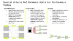
Modern SoC design for artificial intelligence workloads has fundamentally shifted the role of the network-on-chip (NoC) from a simple connectivity fabric to a primary architectural determinant of system performance, power, and scalability. As compute density increases and heterogeneous accelerators proliferate, data movement increasingly dominates overall system behavior. Consequently, NoC architecture must be treated as a first-order design decision rather than a late integration step. The white paper Considerations When Architecting Your Next SoC: NoCs with Arteris emphasizes that modern AI SoCs face bottlenecks not in computation but in arbitration, memory access, and interconnect bandwidth, making NoC topology, buffering, and quality-of-service policies critical for achieving target performance metrics.
AI-centric SoCs differ from traditional designs in both traffic characteristics and integration complexity. Contemporary systems integrate CPUs, GPUs, NPUs, DSPs, and domain-specific accelerators, generating bursty and highly concurrent traffic patterns that are sensitive to contention and tail latency. These characteristics challenge traditional bus-based architectures and demand scalable NoC topologies capable of balancing throughput and latency. Furthermore, advanced process nodes increase wire delays and routing congestion, making physical implementation constraints tightly coupled to architectural decisions. As a result, topology selection must account for both logical hop count and floorplan feasibility, since physically long interconnects may negate theoretical performance advantages.
One of the most consequential architectural decisions in AI SoCs is the coherency model. Hardware cache coherency simplifies programming but introduces coherence traffic and scalability challenges, particularly with snooping and directory mechanisms. Software-managed coherency, by contrast, reduces hardware complexity and allows deterministic accelerator behavior, though it increases compiler and runtime overhead. Dedicated AI accelerators often favor software-managed memory to minimize unpredictable latency, while heterogeneous SoCs typically adopt hybrid approaches to maintain compatibility with legacy CPU clusters. This coherency choice directly influences NoC traffic patterns, arbitration logic, and memory hierarchy organization, demonstrating that interconnect architecture cannot be separated from system-level memory decisions.
Beyond topology and coherency, specialized NoC hardware units are essential for handling mixed workloads. Link-width adapters enable burst absorption and clock domain crossing, reorder buffers preserve transaction ordering across multiple targets, and QoS arbitration logic ensures latency-sensitive traffic is prioritized over bulk transfers. These features help maintain predictable latency under heavy load, which is crucial in AI systems combining control traffic with large tensor data movement. Without carefully designed QoS policies, critical real-time transactions may suffer starvation, leading to performance variability and degraded system efficiency.
Physical floorplanning also plays a major role in NoC design. Centralized interconnects may minimize logical complexity but can create routing congestion and timing closure risks, whereas distributed NoC implementations align better with partitioned floorplans and reduce long wire lengths. Early architectural modeling should therefore incorporate physically plausible assumptions, including clock domains, power partitions, and IP placement. Ignoring these factors often results in late-stage redesigns that increase schedule risk and engineering cost.
A structured methodology for NoC development further reduces implementation risk. Effective design flows begin with traffic modeling and high-level performance analysis, followed by topology exploration, floorplan alignment, pipeline insertion for timing closure, and validation through physical synthesis constraints. Iterative feedback between architectural modeling and physical implementation allows designers to converge on viable solutions before RTL commitment. Automation frameworks such as topology generation tools can further improve productivity, reduce wire length, and enhance latency by embedding floorplan awareness into the exploration process.
As SoCs scale, physical partitioning becomes unavoidable due to power domains, clock islands, and organizational boundaries. Partitioned NoCs must maintain connectivity while supporting isolation, retention, and reset sequences during power transitions. Coordinating these behaviors across domains is complex and must be addressed early to avoid functional and verification issues. Proper planning ensures that the NoC remains operational across low-power states and wake-up sequences without introducing deadlocks or data corruption.
Bottom line: Architecting a NoC for modern AI SoCs requires holistic consideration of traffic patterns, coherency models, topology, QoS mechanisms, physical floorplanning, and power management. Treating the NoC as a system-level design problem rather than a connectivity afterthought enables scalable performance, efficient power usage, and predictable implementation schedules in increasingly complex heterogeneous silicon platforms.
Daniel is joined by Dr. Wally Rhines, CEO of Silvaco, to discuss the Electronic Design Market Data report that was just released. Wally is the industry coordinator for the EDA data collection program called EDMD. SEMI and the Electronic System Design Alliance collect data from almost all electronic design automation companies globally and compile it by product category and the region where sales occurred. It’s the most reliable data for the EDA industry, providing insight into which design tools and IP are in highest demand worldwide.
Wally explains that Q4 of 2025 was another good quarter for EDA, with 10.3% growth compared to last year. Total revenue was $5.5B, placing the industry solidly over the $20B annual run rate for EDA. He also mentions that the last four-quarter moving average shows 10.1% growth, reflecting the continuing demand for EDA software. Dan then explores several details from the current report with Wally. The split between EDA tools and IP is reviewed with significant data suggesting shifts in IP acquisition strategies. The growth rates of the various segments of EDA are dicussed, along with an exception for growth in a particular region. Substantial changes in resolution enhancement orders are also discussed. Worldwide EDA employment is reviewed, which grew 13.8% compared to last year, with total employment now around 71.5K employees.
The views, thoughts, and opinions expressed in these podcasts belong solely to the speaker, and not to the speaker’s employer, organization, committee or any other group or individual.
FPGA prototyping and hardware emulation originated from two independent demands that emerged at roughly the same time, namely, the necessity to implement digital designs in reconfigurable hardware. This was conceivable given the newly introduced field programmable gate array (FPGA) device.
Yet from the very beginning they were driven by different motivations.
Hardware emulation emerged from the need to tame complexity. As integrated circuits grew larger, engineers could no longer rely on simulation alone to validate designs with millions of transistors. Emulation promised to overcome the simulation limitations, still allowing for controlled execution and powerful debugging.
FPGA prototyping, by contrast, grew out of the drive for speed and real-world execution. Its purpose was not primarily to debug signals deep inside the design, but to run the design fast enough to enable meaningful software development, system validation, and application workloads, long before silicon existed.
For decades, these two approaches lived in largely separate universes, shaped not only by distinct technical goals, but also by different engineering mindsets and even cultural identities. Emulation’s mindset sits on the engineer desk, a world of computer-driven waveform analysis and controlled verification workflows. Prototyping, by contrast, belongs to the lab bench, defined by the sensory reality of cables, hardware peripherals, and real-time execution.
The boundary between them has always been somewhat nebulous and poorly defined. Over time, however, market forces, customer demands, and the growing dominance of software-defined systems steadily pushed these paths closer together. Today, emulation and prototyping are no longer isolated disciplines. They coexist under a shared hardware-assisted verification (HAV) umbrella, increasingly complementary in workflows that span functional correctness, performance analysis, power validation, and full software-stack system bring-up.
Understanding how these two worlds rose, diverged, and ultimately began to converge is essential to understanding where verification is headed next.
The Origins of Prototyping: Breadboarding with Wooden Boards
My earliest memories of hardware design verification take me back more than four decades, to an internship I completed at SIT-Siemens in Milan, Italy. At the time, I designed and built a digital clock using discrete TTL logic, a project that became the subject of my doctorate thesis and the culmination of my electronic engineering degree.
Looking back, what is striking is how radically different the landscape was. In those years, design verification was not an industry buzzword. In fact, there was no verification industry at all. There were no standardized methodologies, no dedicated verification engineers, and certainly no sophisticated platforms for pre-silicon validation. Hardware was tested the only way engineers knew how: by physically building it.
Picture: Lauro Rizzatti and his digital clock
The dominant practice was breadboarding—literally constructing prototypes on wooden boards. Nails served as connection nodes. Wires were routed, wrapped, soldered, and adjusted by hand. The process required equal creativity, patience, and perseverance. Later, wooden boards would be replaced by wire-wrap boards, allowing for higher density and more complex routing, still all manual.
Eventually designers would use printed circuit boards populated with sockets and discrete components. This was progress, but it was hardly “rapid.” Each iteration often required new boards, careful assembly, constant troubleshooting, and the reality that debugging meant chasing elusive errors with physical instrumentation rather than inspecting signals with software tools. Prototyping was essential, but it was slow, costly, and highly errorprone. And a fundamental ambiguity always lingered: was the failure caused by the design itself or by the prototype implementation?
Field-Programmable Gate Arrays (FPGAs) to the Rescue
Everything changed with the arrival of the field-programmable gate array.
FPGAs introduced a novel idea: instead of rebuilding hardware every time the design evolved, engineers could map the design-under-test (DUT) directly into programmable silicon. With that shift, testing moved from a dirty-hands discipline—wooden boards, nails, solder, and hammers—to something far closer to a white-glove workflow.
Prototyping became cleaner, faster, and dramatically more scalable.
In many ways, FPGA prototyping was born directly from the hardware designer’s bench. It remained a hands-on, roll-up-your-sleeves craft, but now empowered by re-programmability and speed. Engineers could run real workloads, connect real peripherals, and observe system behavior at near real-time performance.
For the first time, validation could extend beyond synthetic test vectors. Systems could boot operating systems. Software teams could begin development before tape-out. Hardware could be exercised not only for correctness, but for integration realism.
This was the beginning of a new era: one in which verification was no longer confined to signal-level inspection but expanded toward system-level execution.
FPGA prototyping became the bridge between the abstract world of RTL and the concrete world of deployed electronic systems.
Emulation’s Parallel Rise: Debugging Designs Too Big to Simulate
While FPGA prototyping was taking shape on the engineer’s bench as a practical path toward speed, system validation, and early software execution, a different pressure was building elsewhere in the industry.
Designs were exploding in size.
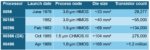
Between the mid-1980s and early 1990s, the semiconductor landscape underwent a structural disruption. Driven by the relentless shrinking of transistor size and dropping cost, integrated circuits (IC) exploded from thousands of transistors to millions. Logic was no longer a series of isolated blocks; it was the entire system, condensed onto a single sliver of silicon.”
Table I: Intel x86 evolution: 1978–1989
Simulation, which had been the workhorse of verification, began to buckle under the weight of this complexity. Not just gate-level simulators, even hardware-description-language (HDL) simulators introduced in the 1990s were becoming increasingly slow. Despite the remarkable progress in compute power, the gap between design size and simulation throughput widened year after year. Furthermore, as designs grew in size, the number of test cycles required to validate them expanded exponentially, stretching the verification schedule beyond tape-out. Comprehensive fault analysis became increasingly out of reach.
It was in this context that hardware emulation emerged—not from the desire to run software fast, but from the need to verify hardware deeply, systematically, and with control. Emulation was born as an answer to complexity.
Two Different Philosophies: Visibility Over Speed
From the beginning, FPGA prototyping and emulation embodied two fundamentally different philosophies. Where prototyping prioritized execution speed and system realism, emulation prioritized control, observability, and debugging.
FPGA prototypes could run rather fast, often at tens or even hundreds of megahertz, but they were notoriously opaque. Once a design was mapped into a sea of programmable logic, internal signals became difficult to access, waveform visibility was limited to compiled internal probes, and debugging required painful recompilation of new or additional sets of probes. Prototyping excelled at-speed execution and early system bring-up, but not necessarily at uncovering the root cause of elusive failures buried deep inside the design.
Hardware emulation, by contrast was conceived as a verification instrument: a specialized platform designed to execute hardware models orders of magnitude faster than simulation, while still preserving the introspection, controllability, and determinism mandatory to carry out debugging quickly and reliably. They were built from the ground up to support the verification workflow. They provided deep signal visibility, full-state capture and replay, non-intrusive tracing, controlled execution with breakpoints, and rapid debug iteration. Their primary purpose was to find and fix bugs, whether deep within complex RTL or at the hardware/software interface, making emulation the natural domain of verification engineers rather than system integrators.
These distinct philosophies were also reflected in operating modes and deployment.
Early emulators often ran in in-circuit emulation (ICE) mode, cabled directly to target systems and driven by real external stimulus. Over time, emulation evolved toward increasingly virtualized environments, integrated with software testbenches, transaction-level models, and hybrid simulation flows. Typical emulation speeds remained in the low single-digit megahertz range—fast enough to escape simulation’s limits but still optimized for observability rather than throughput.
FPGA prototyping, on the other hand, prioritized real-time performance and physical connectivity. It was most effective for designs and subsystems that could fit within a few single-digit FPGAs, enabling extensive software development and interoperability testing long before silicon availability. Prototypes were designed to operate directly with real-world interfaces such as PCIe, USB, Ethernet, and DDR memory, delivering near-system-speed execution.
Organizationally, emulation became a centralized, shared resource: a large platform managed by specialists and accessed by distributed teams of verification and software engineers worldwide for deep-dive debugging and pre-silicon software bring-up. Prototyping, conversely, often lived on the hardware designer’s bench as a hands-on, roll-up-your-sleeves discipline optimized for speed, connectivity, and early system validation.
Separate Markets and Vendor Ecosystems
For many years, these two worlds were served by different vendor ecosystems.
The emulation market was dominated by the large EDA companies, whose platforms were tightly integrated into enterprise verification flows. FPGA prototyping, meanwhile, thrived in a vibrant “cottage industry” of smaller, specialized firms. These companies provided high-performance FPGA boards, mostly used industry standard FPGA compilers, and practical tools aimed squarely at hardware engineers and system developers.
The separation was not only technical, but it was also commercial, cultural, and organizational.
The Commercial Convergence of Emulation and Prototyping
Around 2010, a significant market convergence began to take place. Recognizing the strategic importance of owning the entire HAV continuum, major EDA vendors began acquiring the smaller prototyping players. As a result, the “cottage industry” largely disappeared, and today prototyping solutions are offered primarily by the same three major EDA vendors that dominate emulation.
This consolidation fueled a long-held industry ambition: a single unified hardware platform that could serve both purposes. An ideal “one machine that does both” that could be configured as a high-visibility emulator or a high-performance prototype “with the push of a button.”
Vendors have made real progress toward this vision, with offerings such as Synopsys’s EP-Ready (Emulation and Prototyping) systems, originally announced in 2025. In the spring of 2026 Synopsys then doubled down on this strategy by making all of their hardware systems now ‘Software-defined’.
Even unified platforms still require significant manual effort to transition between emulation-style instrumentation and prototyping-style performance. This highlights a crucial truth: the convergence has been primarily economic and commercial, not yet fully technical.
The fundamental engineering tension persists. The deep, intrusive instrumentation required for effective emulation is often at odds with the non-intrusive, high-speed, real-world operation demanded by prototyping. The “push-button” dream remains elusive because it requires solving this core conflict through advanced automation, smarter compilers, and more seamless workflow integration, challenges the industry continues to confront.
Conclusion: From Wooden Boards to Full-Stack Verification
The journey from wooden breadboards to white-glove verification platforms is more than a technological progression. It reflects how the semiconductor industry itself has evolved, from manual construction to programmable prototyping, through industrial-scale emulation, and now into full-stack system validation.
FPGA prototyping and emulation began as two separate worlds, shaped by different user goals, cultures, and constraints. Over time, driven by the unstoppable rise of software-defined systems and the unprecedented demands of AI-era computing, HAV has outgrown its original purpose.
Verification teams will continue to push the envelope across all software-driven use cases. What was once an elusive goal of performing them on a common HAV platform is steadily becoming reality, one software release at a time. If you are a user of these new software-defined platforms, I am curious how are they working out for you?