Extreme Ultraviolet Lithography (EUV or EUVL) is an advanced semiconductor manufacturing technology used to print the smallest features on integrated circuits (ICs), particularly at leading-edge nodes such as 7nm, 5nm, 3nm, and below. EUV uses light with a wavelength of 13.5 nanometers, which is in the extreme ultraviolet spectrum, enabling much finer resolution than traditional deep ultraviolet (DUV) lithography.
EUV is a critical enabler of continued transistor scaling in the post-10nm era and has become the cornerstone of advanced logic and memory production for companies like TSMC, Samsung, and Intel.
Overview
-
Wavelength: 13.5 nm (compared to 193 nm in ArF DUV systems)
-
Source: High-energy plasma from ionized tin (Sn) droplets
-
Resolution: Enables patterning of features as small as 10nm and below
-
Tools: Built primarily by ASML, the only company currently shipping EUV scanners
Why EUV Matters
As traditional lithography approaches its resolution limits, EUV offers a step-function improvement in imaging capability:
| Feature | DUV (ArF immersion) | EUV |
|---|---|---|
| Wavelength | 193 nm | 13.5 nm |
| Numerical Aperture (NA) | ~1.35 | ~0.33 (High-NA: 0.55+) |
| Patterning Strategy | Multi-patterning | Single or double exposure |
| Resolution | ~36 nm (with SAQP) | ~13 nm (single exposure) |
By reducing the wavelength of light, EUV systems can directly print finer features, improving yield, reducing process steps, and lowering costs at advanced nodes.
History and Development
Origins
EUV was first proposed in the late 1980s by academic and national research institutions (notably in the U.S., Japan, and Europe) as a next-generation lithography (NGL) candidate. Early research focused on plasma sources and multilayer mirrors.
Key Milestones
-
2000s: EUV championed by industry consortia (e.g., SEMATECH, IMEC)
-
2010: ASML delivers first pre-production EUV scanner (NXE:3100)
-
2018: TSMC uses EUV in high-volume manufacturing (7nm+)
-
2020s: Widespread adoption in 5nm and 3nm nodes by TSMC, Samsung, Intel
Key Supporters
-
ASML: Only EUV scanner provider
-
Zeiss: Supplies EUV optics and mirrors
-
Cymer (ASML): Provides EUV light source (Sn LPP)
-
Gigaphoton (Japan): Competing EUV light source R&D
-
Pellicle and resist vendors: JSR, TOK, Merck, etc.
How EUV Works
1. Light Source
-
Laser-produced plasma (LPP) is created by firing a high-power CO₂ laser at tin droplets (Sn), creating plasma that emits EUV light at 13.5 nm.
-
Only about 0.1% of the emitted light is usable, making source power and stability major engineering challenges.
2. Optics and Mirrors
-
Since EUV light is absorbed by air and most materials, the system operates in vacuum and uses mirrors, not lenses.
-
Mirrors are Bragg reflectors, made of alternating molybdenum and silicon layers.
-
Zeiss manufactures these with atomic-level precision.
3. Mask and Pellicle
-
EUV masks are reflective (not transparent) and contain multilayer mirror stacks.
-
A pellicle is a thin protective film placed over the mask to protect it from particle contamination. EUV pellicle development is still a challenge due to heat and transmission constraints.
4. Photoresist
-
EUV resists must be sensitive enough to capture patterns at low doses but robust enough to avoid stochastic defects (e.g., line-edge roughness, missing contacts).
-
Metal-oxide and hybrid resists are under development to meet performance needs.
Technical Challenges
EUV adoption required solving a complex array of physics and engineering problems, including:
-
Source Power
-
Original EUV tools had <10W source power; commercial tools now reach >250W.
-
Power levels directly affect throughput (measured in wafers per hour).
-
-
Mask Defects
-
Reflective masks are difficult to inspect and repair.
-
Mask blank defectivity and pellicle integration remain industry bottlenecks.
-
-
Resist Stochasticity
-
As features shrink, stochastic effects (random variability) in resist exposure increase defect risk.
-
High-NA EUV exacerbates this issue due to smaller process windows.
-
-
Tool Cost and Infrastructure
-
Each EUV scanner costs >$150 million and requires extensive fab modifications (e.g., vacuum chambers, cleanroom upgrades).
-
Only a few companies globally can afford EUV-scale fabs.
-
EUV in High-Volume Manufacturing (HVM)
First Deployment
-
TSMC introduced EUV in its N7+ (7nm+) process in 2019 for limited layers.
-
Samsung deployed EUV in its 7LPP and 5LPE nodes.
Current Use
-
EUV is now widely used for:
-
Contact layers
-
Metal-1 / metal-2 layers
-
Cut masks
-
Via and hole patterning
-
Benefits in Production
-
Reduced multi-patterning complexity (e.g., LELELE or SAQP)
-
Fewer masks, fewer etch steps, faster cycle time
-
Enhanced CD (critical dimension) uniformity and lower variability
High-NA EUV: The Next Leap
ASML is now developing High-NA EUV lithography with a numerical aperture (NA) of 0.55, up from 0.33 in current tools.
Key Benefits
-
Improved resolution (<8 nm features)
-
Enables 2nm and beyond
-
Reduces stochastic variability
Challenges
-
New mask size and format
-
New resists with higher sensitivity
-
New optical and mechanical tolerances
-
Tools expected to cost >$400 million
Timeline
-
ASML EXE:5000 and EXE:5200 High-NA tools expected in pilot use by 2025–2026
-
Target nodes: Intel 18A, TSMC A14 or beyond, Samsung 2nm GAA
Global Impact and Strategic Importance
EUV lithography has become a strategic national asset due to its role in advanced semiconductor production.
-
ASML (Netherlands) holds a global monopoly on EUV tools.
-
Geopolitical sensitivity has led to export restrictions to certain countries (e.g., China).
-
TSMC, Intel, Samsung dominate access to EUV, shaping global chip supply chains.
EUV has also enabled:
-
Leadership in mobile SoCs (Apple, Qualcomm)
-
High-performance computing (AMD, NVIDIA)
-
Advanced memory (SK hynix, Micron)
Future Outlook
EUV is poised to dominate lithography for the next decade and beyond, with expected developments including:
-
Broader EUV adoption across layers and nodes
-
High-NA transition around 2025–2027
-
Stochastic defect suppression through new materials and AI
-
Resist innovation (metal-oxide, molecular, CAR)
-
Multi-beam mask writers and improved pellicles
EUV is not just a tool—it’s a technological and economic inflection point in the future of semiconductor manufacturing.
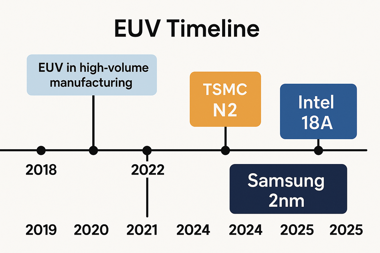
🕰️ EUV Lithography Technology Timeline
| Year | Event / Milestone |
|---|---|
| 1980s | Initial research begins on EUV at national labs (e.g., LLNL, Bell Labs) |
| 1994 | First EUV prototype systems demonstrated by national research consortiums |
| 1997 | EUV LLC (Intel, AMD, IBM + national labs) formed to develop EUV pre-competitively |
| 2001 | International EUV Lithography Symposium begins |
| 2006 | ASML begins developing EUV pre-production systems |
| 2010 | First NXE:3100 pre-production EUV tool delivered by ASML |
| 2012 | TSMC, Intel, and Samsung test EUV for pilot lines |
| 2014 | ASML ships NXE:3300B with improved throughput |
| 2016 | EUV source power exceeds 100W, making high-volume manufacturing viable |
| 2018 | TSMC announces EUV to be used at 7nm+ production (N7+) |
| 2019 | Samsung and TSMC begin volume production using EUV at 7nm |
| 2020 | Intel confirms EUV for 7nm (Intel 4) node |
| 2021 | ASML ships first High-NA EUV prototype tools to partners |
| 2022 | TSMC, Samsung deploy EUV in 5nm and 3nm processes |
| 2023 | ASML introduces NXE:3600D for higher productivity |
| 2024 | Intel, Samsung adopt EUV for sub-3nm production (Intel 3, SF3) |
| 2025 | High-NA EUV systems (EXE:5000 series) enter customer labs for 2nm and below R&D |
https://semiwiki.com/category/lithography/
Share this post via:







Is Intel About to Take Flight?