How Time-Based Scheduling
Reclaims Silicon Wasted by Speculative Execution
By: Dr. Thang Tran, Founder and CTO, Simplex Micro
I have spent my career designing processor architectures, and I have reached an uncomfortable conclusion: a substantial fraction of the silicon area and power in modern high-performance processors exists not to compute results, but to hide from software the fact that instructions execute out of program order.
Out-of-order speculative execution was a necessary engineering choice for an era dominated by general-purpose workloads with predictable branches and abundant independent instructions. Today, the workloads that drive compute investment–AI inference, scientific simulation, and EDA tool execution–have dependency structures that defeat the assumptions of speculative execution. These workloads pay the full cost of speculation machinery while receiving little of its benefit.
The ratification of RISC-V’s RVA23 profile confirms the direction. By making the vector extension mandatory, RVA23 shifts the performance burden from speculative scalar execution to explicit vector parallelism–and in doing so, makes simpler, deterministic scalar cores viable for the first time in mainstream application processors.
Published microarchitecture research documents this overhead consistently. The reorder buffer, reservation stations, register renaming logic, and branch prediction structures together consume an estimated 30 to 50 percent of processor core area in aggressive out-of-order designs. Branch prediction alone accounts for more than 10 percent of total chip power in high-end implementations.
Simplex Micro’s Time-Based Scheduling (TBS) architecture applies this principle to the vector processing unit (VPU), where it matters most for AI workloads. The Simplex CPU is a conventional superscalar out-of-order design; TBS governs the VPU, which executes deterministically and non-speculatively. In the VPU, vector instructions dispatch when their data is ready–not when a predictor guesses they might be ready, not speculatively into a future that may need to be discarded. For AI applications computing many data elements in parallel, speculation would multiply wasted work across every element in the vector. Non-speculative execution is not a constraint; it is the correct architectural choice for this workload class. The silicon recovered from speculation machinery in the VPU can be reinvested in execution units, cache capacity, or core count. These are the resources that determine throughput on the workloads that matter now.
The Problem with Speculation
Out-of-order execution was developed to keep processor execution units busy during data dependency stalls. When instruction B depends on the result of instruction A, a processor that must wait for A before starting B wastes cycles. The out-of-order solution is to look ahead in the instruction stream, find instruction C that does not depend on A or B, and execute C while waiting for A to complete. But implementing out-of-order execution requires four categories of hardware that have no computational purpose–they exist only to support the speculation machinery itself.
The reorder buffer holds instructions that have executed out of program order and tracks them until they can be retired in order, maintaining the architectural illusion of sequential execution. In the Intel P6 family and its descendants, the ROB also stores uncommitted register values, making it a heavily multi-ported structure. Published research characterizes it as “a complex multi-ported structure that dissipates a significant percentage of the overall chip power.” [1] Modern high-performance designs maintain 200 to 500 ROB entries simultaneously, each carrying instruction state, operand values, result data, and status bits tracking whether the instruction has completed speculatively.
Reservation stations hold instructions after decode, waiting for operands to become available. Each cycle, the reservation station logic scans all in-flight instructions, detects ready operands through tag-matching comparisons, and selects instructions for dispatch. This comparison logic fires continuously and scales in complexity with the number of in-flight instructions–not with the number of instructions actually ready to execute.
Register renaming eliminates false data dependencies–write-after-read and write-after-write hazards–that arise when instructions from different parts of the program reuse the same architectural register names within an out-of-order execution window. A processor with 16 architectural integer registers may maintain 180 to 256 physical registers to support renaming, along with rename tables and freelist management. Published analysis confirms: “All contemporary dynamically scheduled processors support register renaming to cope with false data dependencies… the ROB is a large multiported structure that occupies a significant portion of the die area and dissipates a sizable fraction of the total chip power.” [2]
Branch prediction allows the processor to speculatively execute instructions past unresolved conditional branches by guessing the outcome before the branch condition is evaluated. State-of-the-art predictors achieve over 95 percent accuracy but require multiple large prediction tables, branch target buffers, return address stacks, and indirect branch predictors. “High-end processors typically incorporate complex branch predictors consisting of many large structures that together consume a notable fraction of total chip power–more than 10 percent in some cases.” [3]
The published characterization of the aggregate cost is unambiguous: “Out-of-order scheduling logic requires a substantial area of the CPU die to maintain dependence information and queues of instructions… A larger portion of the chip in out-of-order processors is dedicated to issuing instructions out-of-order than to actual execution.” [4] More die area is devoted to the scheduling machinery than to the execution units that compute results. This is the overhead cost of hiding that fact from software.
Itemizing the cost
The Reorder Buffer’s area cost scales with entry count and port count. A 500-entry ROB storing full instruction state and operand values with the multi-porting required for simultaneous read and write access at peak instruction bandwidth is a large SRAM structure. Research published in the Journal of Supercomputing notes that “naive scaling of the conventional reorder buffer architecture can severely increase the complexity and power consumption,” [5] confirming that area scales super-linearly with ROB capacity as designers push for larger instruction windows.
Conservative published estimates place the ROB at 5 to 10 percent of total core area in high-performance designs. Die photo analysis of commercial out-of-order processors–one of the few sources of actual area breakdown data–confirms the ROB as a first-order contributor to core area, accounting for a significant fraction of the identifiable structures. [6]
Branch prediction overhead is the best-documented component because reducing it has been an active research priority for two decades. The published evidence is quantified and consistent:
- High-end processors typically have branch predictors consuming more than 10 percent of total chip power. [3]
- The Alpha EV8 branch predictor alone used 352 Kbits of storage, with “a very large silicon area devoted to branch prediction.” [7]
- Reducing BTB size by a factor of eight achieves 9.2 percent dynamic energy reduction of the processor core. [8]
- A four-wide out-of-order processor’s branch predictor consumes enough power that reducing it by 52 percent reduces overall processor energy by 4.1 percent. [9]
These figures establish branch prediction at 8 to 15 percent of core area and more than 10 percent of core dynamic power in high-performance designs–before accounting for the pipeline flush cost of mispredictions.
Branch prediction overhead extends beyond the predictor structures themselves. When a prediction is wrong, the processor discards all speculatively executed work, flushes the pipeline, and restarts from the correct path. In deep pipelines exceeding 20 stages in modern designs, this flush costs 15 to 30 cycles. Published analysis notes that “around 200 instructions are already executed along the predicted path” before a misprediction is detected and resolved. [10]
For the workloads I target–iterative solvers, simulated annealing, mixture-of-experts routing in LLMs, and dynamic dispatch in EDA tools–branches are data-dependent and misprediction rates are high. The flush cost is paid repeatedly, consuming power and cycles without producing any useful result.
The security cost of speculative execution is precisely documented by production deployments. Spectre and Meltdown, disclosed in January 2018, demonstrated that speculatively executed instructions leave observable traces in processor caches even when their results are discarded–because speculation performs real memory accesses against data the program should not be able to read. The root cause is architectural. Speculation by definition executes instructions before knowing whether they should execute.
Software and microcode mitigations for these vulnerabilities impose measured production penalties:
- Red Hat measured performance impact ranging from 1 to 20 percent across workloads at initial disclosure, improving to 1 to 8 percent with optimized mitigations. [11]
- Intel’s own benchmarks showed 2 to 21 percent degradation on SYSMark workloads. [12]
- I/O-intensive server and database workloads showed 7 to 23 percent degradation. [13]
- HPC workloads running NAMD, NWChem, and HPCC showed 2 to 3 percent single-node degradation, rising to 5 to 11 percent on multi-node MPI configurations. [14]
These are not theoretical costs. They are measured production performance penalties paid by every data center running speculation-based processors, in perpetuity, as the price of a design choice made decades ago. A processor that does not speculate has no Spectre attack surface by construction.
Time-Based Scheduling: The Architectural Alternative
The insight behind TBS is straightforward: track when each instruction’s input data is ready and dispatch it at that moment. Speculation is not needed. There is no requirement to guess at instruction readiness, no need to maintain the appearance of in-order retirement, and no need to search for independent work while waiting on dependencies–the scheduling mechanism resolves all of that directly from operand availability.
TBS tracks operand availability directly. When a producing instruction completes and writes its result, the dependent instruction becomes eligible for immediate dispatch. When operands are not yet available, the instruction waits. No prediction, no speculation, no recovery machinery.
This model eliminates or drastically reduces each of the four speculation overhead categories I described in Section 1:
The reorder buffer is largely eliminated. TBS does not execute instructions out of dependency order–it executes them in data-dependency order, which is the order the computation itself demands. Instructions do not need to be held pending in-order retirement because the commitment model is defined by data availability. Minimal bookkeeping for precise exceptions remains necessary but is a fraction of a full ROB’s complexity and area.
The reservation station shrinks dramatically. Rather than a large centralized structure scanning for ready instructions every cycle through continuous tag-matching, TBS tracks operand availability directly. When a producing instruction completes and its result is written, the dependent instruction is immediately eligible for dispatch. The scheduling logic is driven by completion events rather than polling–architecturally simpler and proportionally lower power.
Register renaming is substantially reduced. False dependencies arise primarily in out-of-order execution where instructions from different program regions execute simultaneously and reuse register names. TBS’s data-dependency-ordered dispatch significantly reduces the occurrence of the write-after-read and write-after-write hazards that renaming exists to eliminate. The physical register file can be substantially smaller than in an aggressive out-of-order design.
Branch prediction is eliminated. TBS does not execute past unresolved branches. When a branch condition depends on an in-flight computation, TBS waits for that computation to complete, then dispatches the correct path immediately. No prediction tables. No branch target buffer for speculative fetch. No misprediction recovery machinery. The Spectre attack surface–rooted in speculative memory accesses along wrong-path instructions–is removed by construction, not by patch.
The aggregate area recovery from eliminating these structures is substantial. Conservative estimates derived from published component figures:
- Reorder buffer reduction: 5 to 7 percent of core area
- Reservation station simplification: 4 to 6 percent of core area
- Register renaming reduction: 4 to 6 percent of core area
- Branch predictor elimination: 8 to 15 percent of core area
Total recovered area: 20 to 35 percent of processor core area, available for reallocation to structures that directly serve computation. In aggressive out-of-order designs where published estimates place total speculation overhead at 40 to 50 percent of core area, the recovery is larger still.
Where Recovered Area Goes
More execution units. A TBS core recovering 25 percent of area from speculation structures can deploy proportionally more arithmetic, load-store, and floating-point execution units. For the workloads I target, more execution units improve throughput directly when the dependency structure permits parallel dispatch–which TBS’s data-readiness model identifies and exploits without speculation overhead.
Larger cache hierarchy. Memory bandwidth and cache capacity are the dominant bottlenecks for LLM inference, HPC iterative solvers, and EDA placement runs. Area invested in larger L1 or L2 caches, or additional cache banks for higher bandwidth, addresses the actual bottleneck rather than overhead the workload never required.
More cores. In a many-core design for parallel workloads–MPI applications, distributed inference, multi-threaded EDA–a simpler TBS core with less speculation overhead means more cores fit on the same die.
On-chip memory. AI inference architectures benefit from large on-chip SRAM scratchpads that reduce off-chip memory traffic. Area recovered from speculation machinery can fund that on-chip memory directly, improving the memory bandwidth situation that limits inference performance more than compute does.
The Power Dividend
Area and dynamic power track closely in CMOS design. Larger structures with more ports consume proportionally more power when active. The speculation machinery that consumes 30 to 50 percent of core area also accounts for a significant fraction of core dynamic power.
Branch prediction’s power profile is particularly significant because the predictor operates on every fetch cycle regardless of whether a branch is encountered. The ROB and reservation stations consume power continuously as comparison logic checks for retirement eligibility and operand readiness. Register rename logic fires on every instruction decode.
Published estimates place speculation-related dynamic power at 20 to 30 percent of core power in high-performance designs. For a processor cluster running continuous workloads–an inference server, an HPC node, an EDA compute farm–20 to 30 percent power reduction translates directly to operating cost over the multi-year deployment lifetime of the hardware.
At data center scale, where power cost over a five-year deployment commonly exceeds hardware acquisition cost, this is a first-order economic consideration, not a secondary specification. I have seen customers plan infrastructure capacity around power envelope more often than around peak compute throughput. TBS addresses both.
Workload Alignment
TBS is not universally superior to out-of-order execution. On workloads with predictable branches and abundant independent instructions–general-purpose integer workloads running operating systems, web servers, and database query engines–speculation machinery provides real benefit and TBS would not automatically outperform it. The crossover point is workloads with deep genuine dependency chains and unpredictable branches. This is exactly the profile of the workloads that now dominate compute investment:
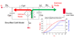
Simplex TBS VPU vs. conventional architectures
Performance, determinism, and silicon efficiency across three architecture classes. Bar length indicates relative advantage–longer is better. Speculative execution cost is measured as estimated pipeline cycles lost to misprediction and flush overhead; Simplex TBS eliminates this category by design. GPU comparison reflects edge-deployment conditions, not datacenter throughput.
LLM inference is a sequential dependency chain by construction. Autoregressive token generation requires each token before the next can be computed. Branch behavior in mixture-of-experts routing is data-dependent and difficult to predict. Speculation machinery provides minimal benefit and pays its full area and power cost regardless. More critically, LLM inference and other AI workloads execute across large vectors of data elements simultaneously. A speculative execution error does not waste one instruction–it wastes work across every element in the vector. The cost of misprediction scales with vector width. Non-speculative, deterministic execution in the VPU eliminates this multiplicative waste entirely.
Scientific computing and HPC iterative solvers–Gauss-Seidel, conjugate gradient, multigrid, simulated annealing–have deep genuine dependency chains where each iteration depends on the previous one. The loop structure is sequential by mathematical necessity. These workloads do not benefit from speculative execution of future iterations because the current iteration’s result determines whether and how the next proceeds.
EDA tool execution–static timing analysis, placement optimization, routing–propagates values through directed dependency graphs where every node depends on its predecessors. The branch behavior during convergence is data-dependent. Speculation machinery works against these workloads rather than for them.
Safety-critical and certified systems represent a fourth category where TBS’s determinism advantage is decisive independent of performance. DO-178C avionics, IEC 61508 industrial safety, and ISO 26262 automotive standards require deterministic, reproducible execution. Speculative execution’s inherent non-determinism at the microarchitectural level is a barrier to certification that cannot be patched away. TBS dispatches in data-dependency order, which is determined entirely by the program and its inputs. The same program on the same inputs follows the same execution path every time. This is determinism by architectural design, not by added overhead.
RVA23 includes Zkt, which mandates constant-time execution for certain operations regardless of data values. This is a determinism requirement in the profile standard itself–one that speculative out-of-order execution makes difficult to satisfy without added overhead, and that TBS provides by architectural design. The same profile makes RVV mandatory, which shifts the scalar core’s role from performance engine to dependency coordinator and makes simple, deterministic scalar execution viable for the first time in mainstream application processors.
Conclusion
The silicon cost of speculation is documented in peer-reviewed microarchitecture research, measured in production deployments affected by Spectre and Meltdown mitigations, and paid continuously in area, power, and security exposure by every data center running out-of-order processors.
The industry accepted this cost for five decades because the benefit was real for the workloads that dominated computing during that era. The workloads that now drive compute investment do not share those characteristics. AI inference, scientific simulation, EDA tool execution, and safety-critical embedded systems all have dependency structures that defeat speculation’s assumptions. They pay the full cost of speculation machinery while receiving little or none of its benefit.
Time-Based Scheduling eliminates that machinery by architectural design. Instructions execute when their data is ready–exactly when the computation’s own logic demands, without speculating when the workload doesn’t require it. The silicon area and power recovered from speculation structures are available for execution units, memory hierarchy, and core count that serve the workload directly.
I designed TBS from first principles about how computation should work when data dependencies are real, sequential, and unavoidable. The Simplex CPU is a conventional superscalar out-of-order design–TBS governs the VPU, which handles the vector-parallel workloads where speculation would be most harmful. The workloads that now dominate compute investment–LLM inference, HPC solvers, EDA convergence–share exactly that structure. TBS is built for them.
Simplex Micro is a RISC-V processor IP company developing Time-Based Scheduling architecture for compute workloads. Specific silicon area and power figures for Simplex Micro’s TBS implementation are available under NDA.
Sources
[1] García Ordaz et al., “A Reorder Buffer Design for High Performance Processors,” Computación y Sistemas, Vol. 16 No. 1, 2012. https://www.scielo.org.mx/pdf/cys/v16n1/v16n1a3.pdf
[2] Kucuk et al., “Complexity-effective Reorder Buffer Designs for Superscalar Processors,” IEEE/ACM MICRO-35, 2002. https://www.academia.edu/18728937
[3] Gao et al., “Efficient Architectural Exploration of TAGE Branch Predictor for Embedded Processors,” ScienceDirect, 2019. https://www.researchgate.net/publication/332775637
[4] ScienceDirect Topics, “Out-of-Order Execution.” https://www.sciencedirect.com/topics/computer-science/out-of-order-execution
[5] Choi, Park, Jeong, “Revisiting Reorder Buffer Architecture for Next Generation High Performance Computing,” Journal of Supercomputing, Vol. 65, 2013. https://link.springer.com/article/10.1007/s11227-011-0734-x
[6] Klauser et al., “Federation: Out-of-Order Execution Using Simple In-Order Cores,” University of Virginia Technical Report, 2007. https://www.cs.virginia.edu/~skadron/Papers/federation_tr_aug07.pdf
[7] Seznec et al., “The Alpha EV8 Conditional Branch Predictor,” 2003. https://www.researchgate.net/publication/3215341
[8] Li et al., “Energy-Efficient Branch Predictor via Instruction Block Type Prediction in Decoupled Frontend,” IET Computers & Digital Techniques, 2025. https://ietresearch.onlinelibrary.wiley.com/doi/full/10.1049/cdt2/3359419
[9] Li et al., ibid.
[10] ScienceDirect Topics, “Speculative Execution.” https://www.sciencedirect.com/topics/computer-science/speculative-execution
[11] Red Hat, “Speculative Execution Exploit Performance Impacts,” 2018. https://access.redhat.com/articles/3307751
[12] InfoQ, “Intel Found That Spectre and Meltdown Fix Has a Performance Hit of 0-21%,” January 2018. https://www.infoq.com/news/2018/01/intel-spectre-performance/
[13] Databricks, “Meltdown and Spectre’s Performance Impact on Big Data Workloads in the Cloud,” January 2018. https://www.databricks.com/blog/2018/01/13/meltdown-and-spectre-performance-impact-on-big-data-workloads-in-the-cloud.html
[14] The Next Platform, “Reckoning The Spectre And Meltdown Performance Hit For HPC,” January 2018. https://www.nextplatform.com/2018/01/30/reckoning-spectre-meltdown-performance-hit-hpc/
Also Read:
Podcast EP340: A Review of the Q4 2025 Electronic Design Market Data Report with Wally Rhines
From Wooden Boards to White Gloves: How FPGA Prototyping and Emulation Became Two Worlds of Verification… and How the Convergence Is Unfolding
yieldHUB Expands Its Impact with New Technology and a New Website