
Digital logic chips synchronize all logic operations by using a clock signal connected to flip-flops or latches, and the clock is distributed across the entire chip. The ultimate goal is to have a clock signal that arrives at the exact same moment in time at all clocked elements. If the clock arrives too early or too late from the PLL output to flip-flop or latch across the chip, then that time difference will impact the critical path delays and the maximum achievable clock frequency. An architect or RTL designer looks at the clock as being a perfectly defined square wave with no delays, while engineers doing timing analysis or physical design know that clock signals are starting to look more like Sine waves than square waves, and that there are delays along the clock tree depending on the topology of the clock network. At small process nodes the On-Chip Variations (OCV) make delays in logic and clock networks differ from ideal conditions, so clock designers resort to adding timing margins.
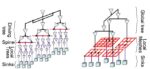
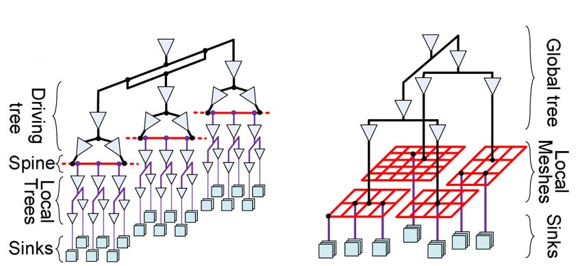
Two popular clock topologies are tree and mesh, so a comparison reveals the differences between each.
| Tree | Mesh | |
| Shared path depth | Higher | Lower |
| Timing Analysis | Static Timing Analysis | SPICE |
| Power | Lower | Higher |
| OCV | More sensitive | More tolerant |
| Clock speed | Lower | Higher |
| Clock skew | Higher | Lower |
| Routing resources | Lower | Higher |
With a tree topology the EDA tool flow is quite automated with Clock Tree Synthesis (CTS) in popular tool flows that include logic synthesis tied to place and route, with timing analysis run on a Static Timing Analysis (STA) tool. The downsides to a tree topology are the sensitivity to OCV, lower clock speeds and higher clock skew. In modern process nodes the aging of P and N channel devices will change the duty cycle of the clock, so it may not be 50% high and 50% low, which then impacts critical path delays.
The mesh topology for clocks provides the highest clock speeds, higher tolerance to OCV and lowest clock skew. A mesh topology has downsides of higher routing resources, higher power consumption and the SPICE requirement for timing analysis. An STA tool cannot be used to analyze a mesh, because with a mesh the clock signal has paths that combine. The only information that a STA tool could provide in a mesh-based clock design is setup and hold analysis, but not critical path analysis.
There is also a middle ground, where the best aspects of tree and mesh topologies are combined, so there are choices for clock topology that are driven by your product requirements.
SPICE circuit simulation using an extracted IC netlist with parasitics is required for timing analysis of mesh-based clock topologies. For accurate analysis of OCV effects a Monte Carlo simulation using SPICE is required, and that is a very time-consuming step, plus your SPICE simulator may not have the capacity for such a large, extracted netlist. If your chip design group is intimidated by using SPICE for analyzing clock timing in a mesh-based topology, then there’s some good news, because the EDA vendor Infinisim has an easy to use product called ClockEdge that is used for clock timing analysis without you having to be a SPICE expert. The analysis provided with ClockEdge will help your team implement a mesh-based clocking topology the quickest, and with the least amount of training.
Summary
SoC designers tackle many technical issues to reach their Power, Performance and Area (PPA) goals, and choosing a clock topology is one of these issues. Most modern chip teams will be attracted to the benefits of using a combined tree and mesh topology for their clock network, as it provides high clock rates, low skew, acceptable routing resources, and withstands OCV effects. The timing analysis of mesh-based clock networks is now simplified by using the ClockEdge tool from Infinisim, as it provides analysis for metrics like: rail to rail failures, duty cycle distortion, slew rate and transition distortion, power-supply induced jjitter.
Related Blogs
- Power Supply Induced Jitter on Clocks: Risks, Mitigation, and the Importance of Accurate Verification
- Clock Verification for Mobile SoCs
- CTO Interview: Dr. Zakir Hussain Syed of Infinisim
- Clock Aging Issues at Sub-10nm Nodes
- Analyzing Clocks at 7nm and Smaller Nodes
- Methodology to Minimize the Impact of Duty Cycle Distortion in Clock Distribution Networks


