#61DAC was buzzing this year with talk of AI and multi-die, heterogeneous design. The promise of making 2.5/3D design and a chiplet ecosystem mainstream reality was the focus of a lot of the panels and presentations at the conference. AI is certainly a driver for this new design style, but the conversation was broader than just AI, as you will see. This new design style will require effort from every part of the semiconductor ecosystem, and this focus was on display during DAC. There is a focal point where all this work needs to come together to make it commercially available. That focal point is the foundry, and there was a keynote address on Tuesday morning at DAC that did a great job explaining how to open the door to the future. Let’s explore how Intel’s Gary Patton shows the way to a systems foundry.
What a Systems Foundry Is and Why It Matters
Before I get into Gary’s keynote, I’d like to address the elephant in the room. I’ve been in the semiconductor business for a very long time. Over the years, I’ve known Intel as a technology powerhouse that dominates markets, crushes the competition and does things the Intel Way.
Open, collaborative, ecosystem-focused and service-oriented weren’t necessarily the first things I would think of when I heard “Intel”. But that’s exactly the presentation delivered by Dr. Gary Patton during his keynote address. Intel is clearly changing, and in a big way. With its systems foundry initiative, Intel is taking a leadership role in defining the future of semiconductor design and manufacturing. This role requires a new type of culture, and Gary is one of the Intel executives that is leading way. I had a chance to speak 1:1 with Gary at DAC, and I’ll share some of his personal insights in a moment. But first, let’s look at some of the messages from his keynote.
Gary began with some eye-opening statistics. According to IDC, the world creates nearly 270,000 petabytes of data every day. That’s 270,000,000,000 gigabytes. Intel estimates that by 2030, 1 petaflop of compute and 1 petabyte of data will be less than 1 millisecond away from the average user. Enabling these achievements will require disruptive innovation – innovation that clearly goes beyond the Moore’s Law scaling we’ve come to rely upon for so long.
He also mentioned that while AI is contributing to this huge growth in data volume and data processing requirements, it also presents significant energy efficiency challenges. According to the NY Times and Google, AI could soon need as much electricity as an entire country (~100 terawatt-hours/year).
Gary pointed out that disruptive innovation is nothing new to our industry. Over the years, we’ve conquered the bipolar power limit, gate oxide limit, and now the planar device limit. Conquering this last one will require a combination of chip and chiplet implementation as well as package interconnect density and energy efficiency. Intel aims to be at the epicenter of all these innovations and that’s what its Systems Foundry initiative is all about.
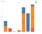
Thanks to its advanced packaging work, Intel is on track to deliver a 50X improvement in energy efficiency and a 10,000X improvement in interconnect density, as shown in the figure below.
Gary looked beyond Intel’s innovations for the complete picture. He discussed the work of UCIe, a consortium of 135 companies. The stated goal of this effort is to develop an open specification that defines the interconnect between chiplets within a package, enabling an open chiplet ecosystem and ubiquitous interconnect at the package level. Gary explained that the work of UCIe is delivering two orders of magnitude improvement in energy efficiency and three to four orders of magnitude improvement in bandwidth when compared with the standard package in the lower left of the figure above. These packaging improvements also deliver at least one order of magnitude lower latency than external interconnects like PCIe, Ethernet etc. This is important work that Intel Foundry is clearly supporting.
Gary then discussed the importance of system technology co-optimization, a much broader and more ambitious version of design technology co-optimization. He explained that software & architecture, packaging, and silicon are all part of this effort which must be holistic. He stated that, “progress at individual layers in the stack is necessary but not sufficient. The entire system must be co-optimized. “
While much of the advanced process and packaging work at Intel is fueling this effort, close collaboration with the entire IP, EDA, design services, and advanced system assembly and test ecosystem is also critical for success. He described in detail the many programs that Intel Foundry has underway with its ecosystem partners to build and certify next-generation design and manufacturing capabilities. He described regular meetings with all key EDA suppliers and showed very detailed scorecards of EDA certifications across all key Intel technologies. The breadth of this effort is truly impressive. Coming a bit later in this post is more proof of Intel’s commitment to an open design flow.
Gary described the five-year investment Intel has made to deliver a systems foundry capability. He reported that today the company has over 100 2.5D designs in manufacturing. Design enablement, an open and collaborative attitude with a quality-first culture and strong customer support and certified methodologies are all part of this investment as shown in the figure below.
The chart above really drove it home for me. This is very much a new and improved version of Intel. One that maintains its technology strengths but adds all the elements of a leading, world-class foundry to create a systems foundry. Next, let’s get to know the presenter of the keynote.
Leading Change – Gary Patton’s Perspective
I was fortunate to have some private time with Gary after his keynote at DAC. Gary is one of the many “outsiders” that Intel has hired over the past few years – that five-year investment that is summarized above. I believe Gary’s entire career prepared him for his current work at Intel. After receiving his Ph.D. in EE from Stanford, he spent over 25 years in various leadership roles at IBM, in research, microelectronics and various corporate initiatives and product lines. Throughout this time, he honed his skills in product/technology development as well as ecosystem collaboration.
He then spent 4.5 years at Globalfoundries as chief technology officer and senior vice president of Worldwide R&D and Design Enablement. He has now been at Intel for 4.5 years as corporate vice president and general manager, Foundry Design Enablement. He is one of the many recent hires at Intel who bring broad industry experience to the company.
Gary explained that he has always had a great respect for the accomplishments of Intel. He came to the company not to “fix” anything, but rather to take a great company to the next level. It seems to have worked out well. He credits the past 4.5 years as the best time in his career. When you consider all the things he’s accomplished, that’s saying a lot.
Gary talked about a corporate-wide shift at Intel to address the broader challenges and opportunities ahead. Tone at the top is an important part of this and Pat Gelsinger is exactly the right person to convey those messages. Gary is delightful to speak with. He is articulate, personable and a very effective leader. A closing comment he made sticks with me. He explained that he brought many lessons learned to Intel from his prior experiences. A key one is that, “if you’re in the foundry business, your customers will make you better.”
Proof of Intel’s Commitment to An Open Design Flow
On the first day of DAC there was more proof of Intel’s growing ecosystem and the commitment being made to create a broad set of reference flows. The following announcements were made by Intel ecosystem partners to support access to Intel’s EMIB technology:
- Ansys is collaborating with Intel Foundry to deliver signoff verification of thermal and power integrity and mechanical reliability of Intel’s EMIB technology spanning advanced silicon process nodes to various heterogenous packaging platforms.
- Cadence announced the availability of a complete EMIB 2.5D packaging flow, digital and custom/analog flows for Intel 18A, and design IP for Intel 18A.
- Siemens announced the availability of an EMIB reference flow for Intel Foundry’s customers. This is in addition to their announcement of Solido™ Simulation Suite certification for custom IC verification on Intel 16, Intel 3, and Intel 18A nodes.
- Synopsys announced the availability of its AI-driven multi-die reference flow for Intel Foundry’s EMIB advanced packaging technology, accelerating the development of multi-die designs.
Suk Lee, vice president for Ecosystem Development at Intel Foundry commented, “today’s news shows how Intel Foundry continues to combine the best of Intel with the best of our ecosystem to help our customers realize their AI systems ambitions.”
You can see the complete announcement from Intel Foundry here. You can learn more about Intel’s plans to deliver a systems foundry for the AI era here. And that’s some backstory about how Intel’s Gary Patton shows the way to a systems foundry. #61DAC