

PieceMakers, a fabless DRAM product company, is making waves in the AI industry with the introduction of a new DRAM family that promises to outperform traditional High Bandwidth Memory (HBM). The launch event featured industry experts, including a representative from Samsung, highlighting the significance of this innovation.
Today, customers are already exploring the use of low-density HBLL RAM for large language models. According to Dr. Charlie Su, President and CTO of Andes Technology, a leading RISC-V vector processor IP provider, “High-bandwidth RAM, such as HBLL RAM, is widely discussed among AI chip makers. When paired with Andes vector processors and customer accelerators, it creates great synergy to balance compute-bound and memory-bound issues.” Eight HBLL RAM chips can deliver a 4 GB density for smaller language models, with a staggering bandwidth of 1 TB per second and at a low cost.
The Need for Advanced DRAM
Since last year, large language models (LLMs) have grown in size and complexity. These models require varying amounts of memory to store their parameters, but one constant remains: the need for high bandwidth. Currently, the landscape of DRAM includes low-power DDR, GDDR, and HBM. However, there is a notable gap in high bandwidth but lower density options, which is where PieceMakers’ new HBLL RAM comes into play.
The name “HBLL RAM” stands for High Bandwidth, Low Latency, and Random Access. Compared to HBM, HBLL RAM offers two additional characteristics that make it superior: low latency and random access capabilities. This innovation addresses the needs of AI applications by providing lower density with high bandwidth.
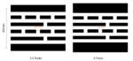
The current generation of HBLL RAM, now in production, offers a low density of 0.5 GB and a bandwidth of 128 GB per second. Future generations are being designed with stacking techniques to further enhance performance. The strategy involves increasing data rate vertically and expanding IO width horizontally. Similar to HBM, HBLL RAM uses 512 IO and data on 1K IO, with future generations set to boost the frequency.
When comparing HBLL RAM to HBM, the advantages are clear. At the same density, HBLL RAM provides much higher bandwidth. Conversely, at the same bandwidth, it offers lower density. This improvement is quantified by the bandwidth density index, which measures the maximum bandwidth per unit density (GB). HBLL RAM significantly outperforms HBM, low-power DDR, and GDDR in this regard.
Bandwidth and Energy Efficiency
Typically, discussions about bandwidth focus on sequential bandwidth. However, the granularity of random access is equally important. HBLL RAM excels in random access performance, outperforming HBM, which has good sequential bandwidth but poor random access capabilities.
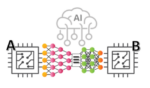
In terms of energy efficiency, HBLL RAM is more power-efficient because it delivers the same bandwidth with a smaller array density or page size. This efficiency stems from its innovative low-density architecture, first introduced at ISSCC in 2017. A single HBLL RAM chip provides 128 GB per second bandwidth across eight channels, with all signal bumps located on one side of the chip. This design results in latency that is approximately half of traditional DRAM, with superior random access bandwidth.
Real-World Applications and Simplified Interfaces
Jim Handy, a respected industry analyst, highlighted HBLL RAM’s potential in an article where he illustrated its placement between level three cache and DRAM. In fact, simulations using HBLL RAM as level four cache yielded impressive results: latency was halved, and average bandwidth increased significantly compared to systems without HBLL RAM.
The simplicity of the memory controller is another advantage, as PieceMakers provides it directly to customers. The interface for HBLL RAM is simple and SRAM-like, involving only read and write operations, plus refresh and mode register set.
One of PieceMakers’ demo boards and a customer’s board exemplify this innovation, utilizing an ABF-only design without CoWos (Chip-on-Wafer-on-Substrate), advanced packaging technology that can be 2-3 times more expensive than traditional flip-chip packaging.Looking ahead, PieceMakers plans to stack HBLL RAM similarly to HBM but without the need for CoWos. This 2D stacking approach, as opposed to 2.5D, promises further cost reductions.
In conclusion, PieceMakers’ HBLL RAM represents a significant leap forward in DRAM technology for AI applications. It offers superior bandwidth, lower latency, and enhanced energy efficiency, making it a compelling choice for future large language models. With the potential to provide up to 128 GB to 16 TB per second, HBLL RAM is set to revolutionize the AI industry.
Joe Ting is the Chairman and CTO, PieceMakers
Also Read:
Unlocking the Future: Join Us at RISC-V Con 2024 Panel Discussion!
Andes Technology: Pioneering the Future of RISC-V CPU IP
A Rare Offer from The SHD Group – A Complimentary Look at the RISC-V Market


