Almost any chip of any complexity contains a control processor of some sort. These blocks are good at executing a wide range of algorithms but there are often two problems with them: the performance is inadequate for some application or the amount of power required is much too high. Control processors pay in limited performance and excessive power in order to get the huge flexibility that comes from programming a general purpose architecture. But for some applications such as audio, video, baseband DSP, security, protocol processing and more, it is not practical just to write the algorithm in software and run it on the control processor. These functionns comprise the dataplane of the SoC.
In many designs that dataplane is now the largest part of the SoC and, as a result, typically takes the longest to design and verify. The design is typically parceled out into several design groups to design and verify their part of the SoC. Meanwhile the software team is trying to start software development but this goes slowly and requires significant rework because the hardware design is not yet available.
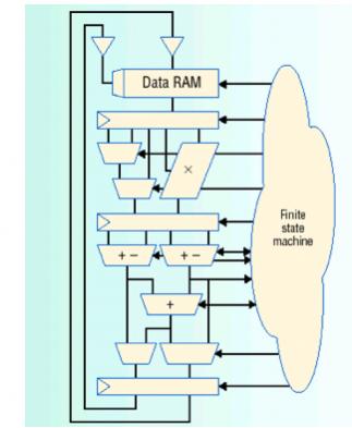
A typical dataplane applilcation consists of the datapaths themselves, where the main data flow, along with a complex finite-state machine (FSM) that drives the various operations of the datapath. Think of a function like an MPEG video decode. The video data itself flows through the datapaths and the complex aglorithms that are used to decompress that data into a raw pixel stream are driven by a comlex state machine off to one side (see diagram).
There are two challenges with this architecture. RTL just isn’t a very good way to describe the complex data operations and as a result it takes too long to create and verify. Secondly, the complex algorithmic nature of the control function is not a good match for an implementation on the bare silicon, since any change, even a minor one, to tweak the algorithm typically requires a complete respin of the chip.
One obvious approach would be to use the control processor to drive the dataplane, but often this does not have enough performance (for high performance applications like router packet analysis) or consumes too much power for simple ones (like mp3 decode). In addition, the control processor is typically busy doing other things and so the only practical implementation requires adding a second control processor
A better approach is to use a dataplane processor (DPU). This can strike the right balance between performance, power and flexibility. It is not a general purpose processor but doesn’t come with a general purpose processors overheads. It is not as hard-wired or expensive as writing dedicated RTL. The FSM can be implemented extremely efficiently but retaining a measure of programmability.
The main advantages are:
- Flexibility. Changing the firmware changes the blocks function.
- Software-based development, with lower cost tools and ease of making last minute changes.
- Faster and more powerful system modeling, and more complete coverage
- Time-to-market
- Ability to make post-silicon changes to the firmware to tweak/improve algorithms
- DPU processor cores are pre-designed and pre-verified. Just add the firmware.
So the reasons to use a programmable processor in the dataplane of an SoC are clear: flexibility, design productivity and, typically, higher performance at lower power. Plus the capabillity to make changes to the SoC after tapeout without requiring a re-spin.
The Tensilica white paper on DPUs is here.