RVN! 26 Banner revised (800 x 100 px) (600 x 100 px)

Why AMD is Up Q4, While Intel is Down

Why AMD is Up Q4, While Intel is Down
by Ed McKernan on 12-19-2011 at 5:45 pm

Immediately following Intel’s announcement that they expected Q4 revenue to come up short by $1B, Rory Read the new CEO of AMD, countered that they were on track to meet their original guidance (see article). Furthermore, “In 1Q and 2Q, maybe you see some manifestations, but I wouldn’t bet against the supply chain,” Read said at a Raymond James conference. “They’re very resilient.” This leads to the question of what is really happening in the PC market and who to believe. My best guess is that Intel decided sometime in November to give up short-term market share for the opportunity to ramp 22nm faster and win back share by mid 2012.

When Seagate reported its earnings the end of November, the CEO mentioned in a Business Week article that at the moment they could take advantage of WD’s shortfall with an immediate 40% increase in hard drive pricing. Alternatively, Seagate would offer customers willing to sign up for one to three years an increase of only 20%. Major PC OEMs were presented with an opportunity that they had not seen in sometime. If they signed on with the new HDD pricing and used an AMD processor, they could gain share with respect to white box PC manufacturers (the ones who would be paying up to 40% more on HDDs). In addition by switching to AMD they would be able to maintain end system price points by offsetting hard drive price increases with the processor price savings. So if it plays out as it has in past history, the branded PC makers should gain share and increased profits this quarter.

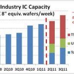
On the Intel side of the ledger, it is likely that the OEMs went to Intel first to appeal for lower processor pricing to offset the hard drive price increases and therefore maintain system price points, especially in the low end consumer market. My guess is that Intel knew that this was coming, however was debating whether to fulfill this quarters numbers or alternatively to focus the company on ramping 22nm faster, getting yields up and driving the ultrabook form factor to the eventual $500 price point sooner rather than later. If one role plays the different scenarios from shortage of HDD in Q1 and recovery in Q2 to the extreme case of full recovery late in Q4, the answer still comes up to ramp 22nm earlier.

Given the above scenario, Intel will now execute on an accelerated Ivy Bridge PR strategy that starts with pre-announcements and system demos starting at the CES show in early January and continuing throughout Q1. This will force a market freeze on many PC purchases in Q1, especially mobiles as consumers wait for the new Ivy Bridge PCs. The market stall will reduce the impact of the HDD shortage and shift the allocation of HDDs in Q1 and Q2 towards systems utilizing the new 22nm Ivy Bridge Mobiles at the expense of all other PCs. Intel’s PR and manufacturing ramp will effectively obsolete a large part of the mobile PC market by sometime in March. System Vendors need to be in synch with Intel or they will lose a lot of money with any overbuilding of inventory that is not sold out prior to the April Ivy Bridge Launch. Intel will also incentivize the retail channel to turn over the floor models overnight. The Intel corporate sales team will inform CIOs that it is best to wait until the new systems arrive. Servers will still be 32nm Sandy Bridge through the 1H 2012.

Just as the rumors of Apple’s iPhone 4S in August and September slowed down the sales of the iPhone4, Intel has the power to cause the PC market to wait for Ivy Bridge’s launch in April. Bottom line is that AMD will enjoy revenue and market share gains in Q4, but beyond that there is great uncertainty. The CES show in January will be very telling. Expect 22nm Ivy Bridge, pre-production notebooks to be widely distributed to press and reviewers so that glowing reviews keep consumers on the sidelines until the official April Launches. The net effect of all Intel’s strategy is that they give up near term revenue and market share to maximize 1H 2012 revenue and get 22nm up the yield curve quicker.

Full Disclosure: I am Long AAPL and INTC


What Will 2012 Bring The Semiconductor Ecosystem?

What Will 2012 Bring The Semiconductor Ecosystem?
by Daniel Nenni on 12-18-2011 at 4:30 pm

During my annual holiday meal with one of my favorite EDA icons some rather bold predictions were made. On his side it was more of what he would LIKE to see happen, on my side it was more of what will HAVE to happen for the semiconductor ecosystem to thrive in the coming years.

Mike Gianfagna (Viva Italia!) spent 15+ years with RCA/GE Semiconductor Division before going to the dark side (EDA). I worked for Mike at Zycad, after that he was a VP at Cadence then eSilicon, CEO at Aprio, and now VP at Atrenta. Mike knows semiconductor design and manufacturing, believe it. Mike also knows wine, is a great visionary, and an excellent lunch date (he paid)!

Foundry Consolidation!

The number of pure-play foundries will continue to decline. 20nm is here and VERY expensive. Intel, Samsung, and TSMC will succeed at 20nm, all others will fail in regards to time-to-market, yield, and/or margins. 450mm is coming in 2015, Intel, Samsung, and TSMC are already building 450mm fabs. The other foundries (GFI, UMC, SMIC) will become what I call boutique foundries like Jazz-Tower and the others. This is all me, Mike predicts you will be able to count the number of foundries below 28nm on one hand, which I also agree with.

Changing EDA Landscape!
Mike commented that the coming process nodes require even tighter integration of design and manufacturing which will pressure foundries to start buying EDA companies. #1 foundry TSMC would acquire #1 EDA company Synopsys and consume the tools for logic synthesis down to mask data preparation. The other parts of Synopsys would be spun out forming a new EDA venture. GlobalFoundries, ever the follower, would then be forced to acquire Cadence and do the same thing. But what about Mentor I asked? This flurry of EDA M&A will get the Carl Ichans of the world excited and they will collectively “roll-up” EDA bits and pieces, including parts of Mentor, into new EDA contenders. What will the new EDA companies look like? According to Mike they will have a much higher level of abstraction in search of new sources of revenue. I guess you would call it EDA180 versus EDA360? Knowing the foundries as I do this is pure fantasy.

Electronic design automation software and semiconductor manufacturing are two very separate and distinct entities, like oil and vinegar. EDA originally spun out of semiconductor manufacturing (IDMs) for this reason. TSMC will never outright buy into EDA because they don’t have to. Instead they will continue to lead EDA with the Open Innovation Program (OIP) and customer pull through. Who are TSMC customers? It would be easier to list the number of companies that don’t work with TSMC. I can’t think of any but I’m sure there is at least one. Even Intel, IBM, and Samung are TSMC customers. GlobalFoundries on the other hand, doesn’t have customer pull though yet, so buying into EDA would be a very big step forward. It would also be fun to watch! Unfortunately with the GFI reorganizations and budget cutting I do not see that happening anytime soon.

The New World Order!
My version of the coming EDA landscape centers around the continued domination of Synopsys, or as one SemiWiki commenter put it “I, for one, welcome my new Synopsys Overlord!” Seriously, who is going to challenge Synopsys now that they have Magma and the largest silicon proven semiconductor IP portfolio? In my humble but expert opinion all of the other EDA minions will continue to fragment until private investment returns and funds a credible resistance. May the force be with us!


Will Rising Smartphone Tide Lift Semiconductor Boats in 2012?

Will Rising Smartphone Tide Lift Semiconductor Boats in 2012?
by Ed McKernan on 12-16-2011 at 5:12 pm

Memo to Self: When all else fails, return to the Smartphone Market!

The announcement by Intel earlier this week that they would come up short this quarter is a reminder that it is not growth, but very high growth that covers a Multitude of Economic Sins (many which are unforeseen). The semiconductor industry has had to endure three major crises this year beginning with the Japan earthquake in March, followed by the Thailand Flood and now the European Sovereign Debt Crises that has already produced a major slowdown across the pond and will impact worldwide growth in 2012. This reminds me of Asia 1997 and Russia 1998 when semiconductor stocks were immediately tossed overboard when fear escalated. They eventually recovered and so in 2012 we should see an upturn in the part of the market that orbits the smartphone.

Intel’s Q4 shortfall was a 4 month delayed response to the Thailand flood that took out more than 30% of the worldwide Hard Drive Industry. In October, the conventional wisdom was that Q4 PC supply was set and that shortages of Hard Drives would not be felt until Q1 2012. However, in the Intel updated earnings call earlier this week, they indicated that OEMs had just finalized their negotiations with HDD vendors and handed Intel a revised forecast. My suspicion is that the HDD vendors upped their prices to the point that PC vendors decided the last 10-20% of volume (in the low end of the market) offered no profit. Intel mentioned in the conference call that OEMs were shifting to higher ASP CPUs – another sign that they are focused more on commercial than retail.

It is clear that there are many moving parts in this story, as Intel highlighted that there would be no wafer cutbacks in Q4. Intel has already begun the shift to 22nm and is likely building ahead inventory in preparation for an April 2012 launch of Ivy Bridge. A true sign of how expensive it is to keep a brand new fab offline. The ramifications of this would seem to say that the die reduction from Sandy Bridge to Ivy Bridge is likely to result in a more aggressive ramp on the ultrabook market. With Ivy Bridge, Intel will also have much more die yield at the 17W TDP ceiling and as a result they can offer lower priced ULV parts. So now it is just a matter of when Intel launches a price war and the marketing dollars to push OEMs towards the $699 price point that is needed to accelerate the mobile conversion away from larger notebooks that may contain AMD and nVidia silicon.

On the OEM side, HP and Dell have made their peace with the fact that they are not going to be players in the consumer tablet or smarphone space. They instead will focus on the corporate side and ride the Wintel Posse in ultrabooks and >$500 tablets that at the very least ensure some profitability. In the end Apple and Amazon have drawn the boundaries around the consumer tablet that will make it difficult for any new entrant that does not sell books, movies and music to go with the tablets.

It is with this market setup that the chip vendors must strategize how best to go forward in 2012 and beyond. Unlike the euphoria of 12 months ago when all ARM based application vendors appeared to be counting on tablets to cannibalize PCs overnight, we are now in a reality where the value has migrated to a new spot – or I should say to two spots. The first area of value-add is no doubt in the baseband chipset. Currently Qualcomm and Broadcom appear to be out executing their rivals and I expect with this will come the bundling of cheap Application Processors. nVidia would differ in this opinion and state that they alone have figured out how to deliver outstanding graphics in a low power applications processor. In 12 months we will know if this is true.

In a research note this week, JP Morgan analyst Rod Hall noted that he expects smartphone unit growth to increase 43% in 2012. This followed the pitch that Broadcom gave to analysts where they saw significant upside to their Q4 revenue based on baseband chipset sales into Apple, Samsung and Nokia (see article). Qualcomm has yet to comment on its Q4 business but many suspect that will also show strong growth. As a side note, Qualcomm and Intel were one of the few suppliers to show >20% growth in 2011 over 2010.

Smartphone vendors will have little leverage over Qualcomm and Broadcom in the coming years because they don’t have the IP or knowledge to replicate the functions. Instead they will focus on the areas that they can commoditize. With the application processor diminishing in value over time and with Samsung and Apple effectively controlling the cost and features of their LCD supply, they are now setting their sights on the one chip that looms large in their Bill of Materials today and even more so in the future – NAND Flash.

Despite all the benefits that the Cloud will produce, one that meets a skeptical eye is the reduction of storage needed on PCs, Smartphones and Tablets. Apple, as an example has recognized that part of the value proposition of the iPhone is the displacement of cameras and video recorders. Therefore on the latest iPhone 4S they upped the camera to 8MP and video to 1080p HD. To make sure the user never came up short on video they increased the NAND storage on the high end to 64GB and set a new, higher price point of $399. Therefore Apple’s iPhone revenues and margins in the future will be partially related to increased camera functionality and reduce NAND Flash BOM.

So perhaps the biggest story this week related to the smartphone industry is the rumored acquisition of Israeli based Anobit by Apple. With Anobit’s Flash Controller technology, Apple can reduce the cost of its NAND flash storage by going out further on the MLC technology curve versus SLC and increase the lifetime of its NAND storage as it scales to lower geometries. This technology would also allow Apple to lower the cost of its MAC Air line relative to the Ultrabook PC copycats. It will be interesting to see how Samsung and Intel respond to the challenge – especially Intel, given that they are an investor in Anobit.


Clock Design for SOCs with Lower Power and Better Specs

Clock Design for SOCs with Lower Power and Better Specs
by Daniel Payne on 12-15-2011 at 5:03 pm

Dan Ganousis posted in our SemiWiki forums about a newer technique to lower the power consumed by GHz clocks on SOC designs and asked if I was interested to learn more, so we met today via WebEx. Dan is with a company called Cyclos Semiconductor, co-founded in 2006 by Marios Papaefthymiou, President and Alexander Ishii, VP of Engineering.
Continue reading “Clock Design for SOCs with Lower Power and Better Specs”


IC capacity utilization declined in 3Q 2011

IC capacity utilization declined in 3Q 2011
by Bill Jewell on 12-14-2011 at 11:54 pm

SICAS (Semiconductor Industry Capacity Statistics) has released its 3Q 2011 data, available through the SIA at: SICAS data . Beginning with 2Q 2011 the SICAS membership list no longer includes the Taiwanese companies Nanya Technology, Taiwan Semiconductor Manufacturing Company Ltd. (TSMC) or United Microelectronics Corporation (UMC). TSMC and UMC are the two largest foundries, with 2010 revenues of $13.3 billion and $4.0 billion, respectively. Losing these companies has caused a major disruption in SICAS data and makes comparison of the 2Q 2011 and 3Q 2011 data with previous quarters invalid in most categories. However TSMC and UMC release information on wafer capacity in their quarterly financial releases. Adding the reported TSMC and UMC data to the SICAS data results in total IC data which is more comparable to prior quarters.

The chart below shows SICAS data for total IC capacity in thousands of eight-inch equivalent wafers per week. Capacity for TSMC and UMC was added to the SICAS 2Q and 3Q 2011 capacity for comparison with prior quarters. 3Q 2011 IC capacity (including TSMC and UMC) was 2,151 thousand wafers, up 3.2% from 2,084 thousand in 2Q 2011 and the sixth consecutive quarterly increase. IC capacity in 3Q 2011 was still 3% below the record capacity of 2,223 thousand wafers in 3Q 2008.

The trend for MOS IC capacity utilization is shown in the chart below. The SICAS data on capacity utilization for MOS ICs excluding foundry wafers was used through 1Q 2011. This data series is fairly comparable to the 2Q and 3Q 2011 SICAS total MOS IC capacity utilization which does not included TSMC and UMC. For the current cycle, utilization peaked at 95.7% in 2Q 2010 and has been gradually declining since, reaching 91.7% in 3Q 2011. Utilization in 3Q 2011 was still higher than the 90.7% in 1Q 2008 prior to the industry downturn. In general, utilization above 90% is healthy for the IC industry.

What is the outlook for MOS IC capacity utilization in 4Q 2011 and in 2012? This depends on the rate of capacity increase and the level of shipments. Although capacity has increased for 6 consecutive quarters, signs point to a flattening or possible decline. TSMC expects its 4Q 2011 capacity to be flat with 3Q 2011. The chart below shows three-month-average semiconductor manufacturing equipment bookings and billings from SEMI (U.S. & European companies) and SEAJ (Japanese companies). After a sharp falloff, bookings and billings began to recover in the second half of 2009, leading to capacity increases beginning in 2Q 2010. Bookings peaked in August 2010 and billings peaked in May 2011. October bookings were down 39% from the peak and billings were down 21% from the peak. The equipment data indicates capacity growth should slow down significantly in the next few quarters.


Shipments of IC wafers could be flat to down in 4Q 2011, based on WSTS data and recently lowered revenue guidance from Texas Instruments and Intel. Thus even with close to flat capacity growth in 4Q 2011, MOS IC capacity utilization will like drop from 91.7% in 3Q 2011 to close to 90% in 4Q 2011. In 2012, capacity growth will remain slow for at least the first half of the year. Semiconductor market growth in 2012 (and IC wafer shipments) is expected to be stronger than in 2011. The result should be MOS IC capacity utilization remaining above 90% for at least the first two quarters of 2012.


MEMS layout and automation

MEMS layout and automation
by Daniel Payne on 12-14-2011 at 11:12 am

At a webinar today I listened and learned about how a tool called L-Edit can be used to layout MEMS designs plus automate the task to be more productive. I can see how the history of IC layout editing is now being repeated with MEMS because in the earliest IC layout tools we could only do manual entry of polygons, then gradually we got cells with hierarchy, then automation with placement, and finally parameterized cells.

I’ve attended dozens of webinars however this was the first one where we used Adobe Connect as the web conference software. What impressed me was that I could just use my standard web browser to see and hear the webinar, I didn’t have to install something, calibrate, run tests, or in general panic because my computer wasn’t setup with prerequisites. The feedback as an attendee was only thru a text window, so we didn’t use microphones during the Q&A. I prefer the simplicity of this webinar technology to others where I have to use my cell phone as a separate audio channel to listen.

John Zuk started out the event with an intro to who Tanner EDA is, there history since 1988, Tanner MEMS does consulting in the MEMS area for clients.

Customers using Tanner for MEMS include: InvenSense, AMFitzgerald, MEMSIC, Knowles, SmartBead, Hymite.

There are many companies offer tools for MEMS layout, so why choose Tanner? Their tools look easy to learn and use, are integrated with popular formats, work with foundries, and have a low cost of ownership.

MEMS Demo
Thuong U ran the L-Edit tool to demonstrate some of the features for doing MEMS layout:

  • Does both MEMS and IC layout
  • Technology is configurable
  • Supports hierarchy
  • Design navigator
  • Customizable keyboard, palette and rulers
  • User and workgroup configurations
  • Has a command line interface
  • Supports GDSII, CIF, EPS and DXF formats
  • User properties on layout objects
  • User Programmable Interface – using C code
  • Cross-section viewer
  • Advanced editing support

We saw a magnetic MEMS actuator used in the demo, along with creating cells from scratch. The colors used in L-Edit show you all the layers for a design, in contrast to AutoCAD.

With L-Edit you can draw: boxes, polygons, all-angles, circles, pie wedges, toroids, convert edges into curves either concave or convex. On the automation side you can even select a layout object then perform boolean operations on it to create a new version of the object by growing and shrinking by a set amount.

Object snapping made layout operations automatically snap to a vertice, edge, mid-point or intersection. This was similar to the AutoCAD snapping feature.

A base point is used like the AutoCAD tracking point feature. The L-shaped object below was used to show how you can select a vertice as a base point, then transform the object from that selected point.

Many of the editing commands have shortcuts that sounded intuitive like R for rotate and D for duplicate.

In the IC world we’ve had Design Rule Checking (DRC) for decades however in the MEMS world this is an emerging concept and feature that L-Edit has. When DRC was run on the Magnetic Actuator it found a handful of spacing and width violations that could then be pinpointed and corrected.

AutoCAD uses DXF file formats and you can import/export these with L-Edit:

On the export side you can go out to GDSII for fabrication or PostScript as a negative or positive maks layer for transparencies.

With the User Programmable Interace (UPI) you can automate layout commands using C code and even extend the GUI. SoftMEMS has written code to show 3D cross-sectional viewing as an add-on to L-Edit.

There’s even a feature to automatically create text on a layer:

Q&A
Q: Can you do arrays?
A: Yes, just place an instance of any cell, select it, Control E, then choose your array parameters. You can also Edit-in-Place with any cell instance.

Q: How about parameterized cells?
A: Yes, you can write these with T-Cells in C code. Here’s a concentric Toroid example with T-Cells. Instantiating a T-Cell uses a built-in C compiler.

Q: What tools does Tanner offer for MEMS?
A: Two choices: L-Edit MEMS (L-Edit plus import/export of DXF, curve tools), L-Edit MEMS Design (previous plus DRC).

Q: Can you flip or mirror about an axis that is not vertical or horizontal?
A: Yes, you can rotate a selected object by an arbitrary angle.

Q: What OS is supported?
A: Both Windows and Linux are supported for L-Edit.

Summary
Tanner EDA has a capable MEMS layout tool in L-Edit with a growing number of customers and also uses its own tools as part of a consulting business. There are many MEMS layout tools to consider (AutoCAD, Coventor, softMEMS, SolidWorks, Cadence Virtuoso), so add Tanner’s L-Edit to your evaluation list.


iLVS: Improving LVS Usability at Advanced Nodes

iLVS: Improving LVS Usability at Advanced Nodes
by glforte on 12-13-2011 at 4:54 pm

LVS Challenges at Advanced Nodes

Accurate, comprehensive device recognition, connectivity extraction, netlist generation and, ultimately, circuit comparison becomes more complex with each new process generation. As the number of layers and layer derivations increases the complexity of devices, especially Layout Dependent Effects (LDE), becomes harder and harder to model. One of the keys to design success in 40nm and 28nm is to enable customers to easily modify foundry rule deck to include their own device models for transistors, resistor, capacitors, inductors, etc., and even augment the deck with their own checks.

iLVS—A More Standardized Approach

To address this situation, TSMC and Mentor Graphics have collaborated to define iLVS, a syntax that provides customers with a more easily adaptable solution to their circuit verification needs. Using iLVS, users can more easily modify and augment foundry rule decks, yet still adhere to the modeling and manufacturing intent captured in these decks.The goals of iLVS are to improve technology data integrity while reducing duplicate development effort. iLVS supports multiple EDA tools, which makes it easier for customers to adopt new EDA vendor innovation in the form of optimized tool implementations. It also makes it possible for customers to take advantage of these innovations and enhancements earlier. At the same time, iLVS makes it easier to customize LVS rule decks to accommodate users’ own unique device definitions or to introduce specialized checks.

iLVS Architecture

An iLVS rule deck is implemented with the Tcl scripting language, which calls a set of standardized library functions that are common across different tools. The library is a superset of the most commonly used LVS operations. At the implementation level, each tool vendor implements the standard functions using the tool’s native language syntax. This allows vendors to optimize the executable code for best accuracy and performance, while shielding the rule deck developer from the details of the tool implementation.iLVS is non-intrusive in that it can be introduced without changing the user’s current design methodology and flow. Everything a user needs to adopt iLVS—the TSMC iLVS rule deck, the standard functions library, and the vendor implementation library—is available as a package download from TSMC.

Transitioning to iLVS

To make it easier for users to define their LVS devices, iLVS uses a device truth table to add and modify devices. This typically simplifies the rule deck by converting many Boolean functions into a single truth table for a class of devices. It also makes the deck easier to maintain. To enable a smooth transition from existing LVS decks to iLVS, the syntax allows customization through “in-line” calls to unique tool functions. In this way the majority of LVS checks can be handled by standard iLVS syntax, while a user’s unique operations can be maintained in the same deck. Specialized electrical rule checks can be handled in this manner for example.iLVS decks are now available from TSMC for 65GP, 65LP, 40G, 40LP, 28HP, 28LP, 28HPM and 28HPL processes, and 20G is in the development pipeline.

Authors: Carey Robertson, Mentor Graphics and Willy Chen, TSMC

This article is based on a joint presentation by TSMC and Mentor Graphics at the TSMC Open Innovation Platform Ecosystem Forum. The entire presentation is available on line on theTSMC web site (click here).


IP-SoC 2011 Trip Report: IP again, new ASSP model, security, cache coherence and more

IP-SoC 2011 Trip Report: IP again, new ASSP model, security, cache coherence and more
by Eric Esteve on 12-13-2011 at 9:05 am

For the 20[SUP]th[/SUP] anniversary of IP-SoC, we had about ten presentations, most being really interesting; the conference has provided globally a very good level of information, speakers coming from various places like China, Belarus, The University of Aizu (Japan), University of Sao Paulo (Brazil), Silesian and Warsaw University of Technology (Poland), BNM Institute of Technology (Bangalore-India) and obviously from western Europe and USA. I am going to IP-SoC for more than five years now, and I am glad to see that there is no more room for the insipid “marketing” presentation that some IP vendors used to give. It was real information, and if you were attending to presentation focused on security, like this given by Martin Gallezot (one of my former colleagues at PLDA), you really needed to know a bit on the topic (Physical Attacks against Cryptographic) to fully understand… but that’s exactly what you expect when you go to a conference, isn’t it? Learn something new for you.

And, obviously, doing networking within this niche part of the industry which is IP. IP-SoC was the right place to network, and I did it as much as possible, as well as finding new customers in the IP vendor community. Sorry, I can’t give you names; we need to close the deal first!

Starting with the 20th anniversary Special Talk, we had (as usual) a « Semiconductor design IP Market overview » from Gartner ; if you remember my blog in January about Gartner, they were very good at forecasting… the past. This year, Gartner has improved, as they are now giving a year-to-year design IP revenue growth forecast of 10% for 2011, 4% for 2012, and 8% for 2013 and later, which is more on line with what we can expect from the IP market, compared with the few % they gave last year. Also interesting, the result of a survey made by Gartner with the IP consumer. In particular:

  • To the question: “What are the most important criteria to select a specific IP?” 90% have answered “It must be Silicon provenand tested”.
  • To the question: “Why do you use design IP?” 70% have answered “To improve Time-To-Market”.

Nothing surprising in these answers, but rather the confirmation that it’s really difficult to enter the IP market, as even if your product is wonderful, it will not be silicon proven, and the first sale will be very difficult to make!

The conclusion from Gartner was, at least to my opinion, rather funny: “78% of the semiconductor growth in 2012 will come from Smartphone and Media Tablet; so you should sell on this market”. Funny, because if you are not selling on this market, it’s probably too late in December 2011 to modify your port-folio to attack it in 2012…

Last information you may value: IP market weighted $325M in 1998, and weights now $1.7B; this represent 0.12% of the value of the End Equipment served by these IP; impressively low, isn’t it?

Another presentation http://www.design-reuse.com/ipsoc2011/program/ was by Marc Millerfrom Tabula. I know Tabula (and Marc) since 2005, when we decided at PLDA to support them with our PCI Express IP. At that time, only a few people did really understood what exactly their product was. I think in the meantime, a lot more people understand Tabula new concept, based on “dynamically reconfigurable hardware logic, memory, and interconnect at multi-GHz rates”. That’s a pretty good idea: the same piece of Silicon, say a LUT as we are in the FPGA world, will be used to support different logic functions, within the same system clock period! Two remarks: at first, the Silicon should run as fast as possible, that’s why Tabula has invested into 40nm technology; second remark: how damn can we use the existing design (EDA) tools? The answer is: no way! So, Tabula is 50% an EDA company, designing his own toolset, and 50% a hardware FPGA vendor. According with Marc, the “official” release of the tools is to come very soon, I say “official” as Tabula is already claiming to have customers. Will Tabula successively compete with the duopole? I don’t know, but their product is real innovation!

I realize that one blog is too short to cover all the other interesting presentations (cache coherence, 3D-IC for butterfly NoC to name a few), I will have to come back in a second blog. I will just mention… my presentation before leaving you: Interface IP Market Birth, Evolution and Consolidation, from 1995 to 2015. And further?”That was the first time I saw people standing during the show, not to leave the room but to better see the slides! Among a few compliments I got after the presentation, one was especially precious to me, as it came from a SC, and even IP, veteran: Jonathan Edwards, now IP Manager at ST-Ericsson. In fact, Jonathan started his career back in the 70’s working with GEC Plessey then INMOS in the UK, and for ST-Microelectronics when they bought INMOS, and has stayed in the technical expertise role all time long. Thanks again Jonathan!

By Eric Estevefrom IPnest– Interface IP Survey available here.


Learning About MEMS

Learning About MEMS
by Daniel Payne on 12-12-2011 at 6:34 pm

My automobile has an air bag system that uses a MEMS (Micro Electro Mechanical System) sensor to tell it when to deploy, and I’ve read headlines talking about MEMS over the years so I decided it was about time to learn more by attending a Webinar on Wednesday, December 14th at 8AM Pacific Time.

The EDA company hosting the Webinar is Tanner EDA and I’ve read specific customer examples about MEMS design in four different applications:


Hymite – MEMS packaging


Knowles – Microphone

What I’ve learned so far about MEMS:

[LIST=1]

  • You can write macros in C or C++ to control your MEMS layout in the L-Edit tool, and they’re called T-Cells. Reminds me of Cadence Pcells or other IC layout approaches like PyCells.
  • Some MEMS chips need to be hermetically sealed in order to function properly.
  • Arcs and circles are typical MEMS layout shapes, unlike most IC designs that are strictly rectangular in shape.
  • Visuallizing MEMS layout in 3D helps shorten product development times.
  • Accelerometers are what goes into the airbag system and MEMS are ideal for this application.
  • MEMS can be used to barcode micro-particles used in medical testing.
  • The realms of IC design and Mechanical design still use separate analysis software but common layout tools.

    After the webinar on Wednesday I’ll blog about what I’ve learned.


  • View from the top: Ajoy Bose

    View from the top: Ajoy Bose
    by Paul McLellan on 12-12-2011 at 4:13 pm

    I sat down yesterday with Dr. Ajoy Bose, CEO of Atrenta, to get his view of the future of EDA – looking through a high-power “spyglass” of sorts. I first met Ajoy when he was at Software & Technologies. I was then the VP of Engineering for Compass Design Automation and we were considering off-shoring some development. We eventually dipped a toe in the water with small groups in both India (at Hyderabad) and Moscow. The feel of India from inside a high-tech company building is very different from the feel outside on the street, but that’s a story for another day.

    Ajoy believes that what Cadence calls SOC Realization in their EDA360 white paper is a transformation of how design is done that is as great as the move from schematics to RTL, although just as then, it is a transformation that takes years to complete.

    We talked about the fact that chips are no longer really designed at the RTL level – they are assemblies of IP blocks. But IP quality and other design meta-data is lacking in standard representations in the design flow, which is getting to be a big problem. Hmm, sounds like the interoperability forum I was at earlier in the week.

    Ajoy believes the Holy Grail is early exploration, making sure a design meets its targets for power, performance and area well before you commit to detailed implementation. This process requires more collaboration within the ecosystem, along with standards for IP creation, IP assembly and SoC assembly. One opportunity is solving problems early and only once in the design cycle, which requires additional information in the form of constraints and waivers.

    We also talked about the fact we need a much better way to abstract a block. For physical design, we can take a block and “black-box” it, just needing to know where the terminals are. But for IP blocks it’s not that easy. You can’t do IP-based design the way you used to be able to take your TI 7400 series databook and do printed circuit board design. IP doesn’t work like that for timing, or for testability. Much more detailed information needs to be processed to get a useful answer. The same is true for power consumption.

    Of course another big change is that software forms more and more of the design. This is seen most clearly at Apple where software is the king. Apple builds chips especially optimized to run exactly the required software load.

    Ajoy reckons that about 10% of design groups are taking all this into account and doing design that starts with the software and then designing the hardware using the software to focus that development. The other 90% design the chip and then let the software guys have at it, which is much slower and less predictable.

    From an EDA business point of view it is clear that the system companies are taking more control. These types of companies seem to be prepared to pay for tools that deliver value. Since they are not already making enormous purchases of less differentiated stuff they seem less inclined to insist that everything is simply rolled into an all-you-can-eat deal for next to nothing.

    There is a chance that design handoff will move to this block level, the level that specifies the virtual platform for the software people and the IP to be assembled for the SoC team. It is still early, but Ajoy and Atrenta believe the change is coming.