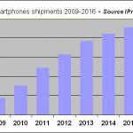
100X800 Banner (1)

HP Will Farm Out Server Business to Intel

HP Will Farm Out Server Business to Intel
by Ed McKernan on 09-04-2011 at 7:36 pm


In a Washington Post Column this past Sunday, Barry Ritholtz, A Wall St. Money Manager and who has a blog called the Big Picture, recounts the destruction that Apple has inflicted on a wide swath of technology companies (see And then there were none). He calls it “creative destruction writ large.” Ritholtz though is only accounting for what has occurred to date. I would contend that we are about to start round two and the changes coming will be just as significant. If I were to guess, HP will soon decide to Farm out its Server Business to Intel. Intel will soon realize that they will need to step up to the plate for a number of reasons.

When HP hired Leo Apotheker, the ex-CEO of Software Giant SAP, the Board of Directors (which includes Marc Andreessen and Ray Lane, formerly of Oracle) implicitly fired the flare guns that they were in distress and were going to make radical changes as they reoriented the company into the software sphere of the likes of Oracle and IBM. To do this, they had to follow IBM’s footsteps by first stripping out PCs. IBM, however, sold its PC group to Lenovo back in 2004 before the last downturn. Unfortunately for HP, it will get much less for its PC business than what they paid for Compaq.

The next step for HP is risky but necessary. They need to consolidate server hardware development under Intel. Itanium based servers are selling at a run rate of $500M a quarter at HP are now less than 5% of the overall server market compared to IBM Power and Oracle SPARC, which together account for nearly 30% of the server dollars. Intel and AMD x86 servers make up the rest (See the chart below). In addition, IBM’s mainframe and Power server businesses are growing while HP’s Itanium is down 10% year over year.

Oracle’s acquisition of Sun always intrigued me as to whether it was meant as a short-term effort to force HP to retreat on Itanium or as a much longer-term strategy of giving away hardware with every software sale. When Oracle picked up Sun, it still held a solid #2 position in the RISC world, next to IBM. By taking on Sun, Oracle guaranteed SPARC’s survival and at the same time put a damper on HP growing more share. New SPARC processors were not falling behind Itanium as Intel scaled back on timely deliveries of new cores at new process nodes. More importantly, the acquisition was a signal to ISVs (Independent Software Vendors) to not waste their time porting apps to yet another platform, namely Itanium. Oracle made sure that HP was seen, as an orphaned child when it announced earlier this year that is was withdrawing support for Itanium.

There is only one architecture, at this moment, that can challenge SPARC and Power and it is x86. It is in HP’s interest to consolidate on x86 and reduce its hardware R&D budget. If needed, a nice software translator can be written to get any remaining Itanium apps running on x86. Since the latest XEON processors are three process nodes ahead of Itanium, there should be little performance difference. But what about Intel, do they want to be the box builder for HP?

I would like to contend that Intel has to get into the box business and is already headed there. There chief issue in holding them back is the reaction from HP, Dell and IBM. Neither of them is generating great margins on x86 servers. With regards to Dell, Intel could buy them off with a processor discount on the standard PC business, especially since they will now be the largest volume PC maker. IBM is trickier.

But why does Intel want to go into the server systems business. The answer is several fold. From a business perspective they need more silicon dollars as well as sheet metal dollars. Intel sees another $20-$30B opportunity in ramping up and they will need it to counteract any flatness or drop in processor business in the client side of the business. Earlier this year, Intel bought Fulcrum, if they build the boxes for the data center, then they have the potential to eat away at Broadcom’s $1B switch chip business.

A more interesting angle is the data center power consumption problem. Servers consume 90% of the power in a data center. It used to be that processors were the majority of the power, but with the performance gap growing between processors and DRAM and the rise of virtualization it now becomes a processor and memory problem. Intel is working on platform solutions to minimize power but they expect to get paid for their inventions.

Intel has started to increase prices on server processors based on reducing a data center’s power bill. Over the course of the next few years they will let processor prices creep up, even with the looming threat of ARM. This is a new value proposition that can be taken one step further. If they build the entire data center box with processors, memory, networking and eventually storage (starting with SSDs), then they can maximize the value proposition to data centers, who may not have alternative suppliers.

In some ways Intel is at risk if they just deliver silicon without building the whole data center rack. There are plenty of design groups at places like Google, Facebook and others who understand the tradeoffs of power and performance and would like to keep cranking out new systems based on the best available technology. By Intel putting down its big foot, it could eliminate these design groups and make it more difficult for a new processor entry (AMD or ARM based) from entering the game.


I love you, you love me, we’re a happy family…

I love you, you love me, we’re a happy family…
by Paul McLellan on 08-31-2011 at 8:00 pm

The CEO panel at the 2nd GTC wasn’t especially enlightening. The theme was that going forward will require cooperation for success and everyone was really ready to cooperate.

The most interesting concept was Aart talking about moving from what he called “scale complexity” aka Moore’s law to what he called “systemic complexity” where we are moving from the age where transistors are cheaper at each process generation to where you can build larger systems, but the per transistor cost will not be less.

Aart also had the most memorable image of the afternoon. He was talking about how amazing it is that you go to a fine-dining restaurant with 8 people and course after course things come to the table at the same time all perfectly prepared. My daughter’s boyfriend is the chef of just such a restaurant so I know about it a bit from behind the scenes and it is still amazing. Delivering a foundry capability is like that: the process, the tools, the IP, the manufacturing ramp and everything else needs to all be ready at the same time. The output isn’t the sum of the factors but the product, and if one is zero the whole thing is a big zero. Global Foundries’ kitchen just happens to cost billions of dollars, a bit more than even the most over the top fine dining restaurant.

Mojy, who was chairing the session, had one question to try and break up the love-in. Global Foundries, IBM and Samsung all compete, and yet they cooperate in process development even going as far as fab-same implementation (same equipment etc in all the fabs of each company). Will the big EDA companies cooperate in the same way? Of course this is a bit of an unfair question. The only reason that semiconductor companies cooperate is that technology development has got too expensive for any one company (except Intel, always the exception) to do it alone as they would have done 15 years ago (and, indeed, did). While foundries and semiconductor companies get some differentiation through process, most comes from what they design (for IDMS) or how they service customers operationally (for foundries). The software that EDA companies create is their differentiation. If Cadence, Synopsys, Magma and Mentor cooperated to build a shared next generation place and route system then it is hard to see how they would differentiate themselves. Yes, some companies have better AEs, some have better geographic coverage in some places etc, but basically they would all be selling a product that they could only differentiate by price. Today, with unique systems but with broadly similar capabilities, they are already close to that situation. So the CEOs largely ducked the question since “no” would have been too direct an answer.


Global Technology Conference 2011

Global Technology Conference 2011
by Paul McLellan on 08-31-2011 at 7:07 pm

I went to the second Global Technology Conference yesterday. It started with a keynote by Ajit Manocha who is the CEO of about 2 months. I hadn’t realized until someone asked him during the press lunch that he is technically only the “acting” CEO. Actually, given his experience he might be the right person anyway, rather than just a safe pair of hands in the meantime. He was Chief Manufacturing Officer for NXP (nee Philips Semiconductors) and so already has, as he put it, experience of running multiple fabs in multiple countries. When asked if he might become the permanent CEO he basically said that he’d advised the board to look for the best person possible. And then he added that, of course, if he didn’t deliver he’d be out of a job anyway.

Ajit (and everyone at Global) makes a big deal about being globally distributed as opposed to clustered in one country like any companies using the “traditional model”, such companies going unmentioned as if the mere mention of TSMC might lose business (oh, wow, I didn’t know you had a competitor, I must give them a call). Of course the tsunami in Japan has made people more aware of how vulnerable supply chains are sometimes, and of course Taiwan also sits in earthquake country, not to mention political instability country if China’s leaders decided to do something stupid. Global tries to have every process (the recent ones, anyway, the old ones are only in the old Chartered fabs in Singapore) in at least two of their fabs (Singapore, Dresden in the old East Germany, and the one under construction in upstate New York which is now ready for equipment install ahead of schedule).

Ajit talked mostly about getting closer to customers and being the vendor choice. Of course at some level everyone tries to do that and it is much easier to talk about than it is to achieve in practice. But here are a few interesting statistics: over 150 customers, over 11,000 employees and spending $8B on capex 2010-2011.

The capacity they have in place is quite impressive. Fab 1 (the old AMD fab in Dresden) is expanding to 80,000 wafer starts per month. I assume that means 300mm wafers rather than 200mm wafer-equivalents that is sometimes used. The focus is 45/40/32/28nm. Fab 8 (under construction in New York) is big: 6 football fields of clean room with over 7 miles of overhead track for moving wafer transport vehicles around. It will have 60,000 wafer starts per month once ramped, focused on 28/20nm. And in Singapore (the old Chartered fabs) they have a lot of 200mm capacity and, in fab 7, 50,000 wafer starts per month anywhere from 130nm to 40nm.

The meat of what Global is up to was in Gregg Bartlett’s presentation on the implementation of their process roadmap. He is very proud that they have gate-first 32nm HKMG ramped while other people using it are struggling. During the lunch he was asked about Intel’s 3D transistor. He thinks that despite some advantages, they will prove very difficult to control in the vertical dimension and are too restrictive for a general foundry business. Which is interesting if true since Intel has more capacity than it needs and so is entering the foundry business!

At 28nm they will use basically the same FEOL (front end of line, i.e. transistors) as at 32nm, namely gate-first HKMG. Compared to 40nm this is a 100% density increase and either a 40% increase in performance or a 40% reduction in power (depending on how you take it). He reckons that die are 10-20% smaller relative to 28nm gate-last processes. That would be TSMC.

But apparently at 20nm, litho restrictions mean that you can no longer get that 10-20% benefit so they will switch to gate-last. Versus 28nm this is nearly a 50% area shrink and they are investing in innovation in interconnect technologies.

And after that? 16/14nm. Multi-gate FinFET transistors, lots of innovation. Also innovation in EUV (extreme ultraviolet) where they have been doing lots of development work (over 60 masks delivered) and will have production installation in New York in the second half of next year.


Economic news not all bad for semiconductors

Economic news not all bad for semiconductors
by Bill Jewell on 08-30-2011 at 2:06 pm


The economic news lately has been bleak. U.S. GDP grew at an anemic 0.4% in 1Q 2011 and 1.0% in 2Q 2011 – leading to increased concerns about a double-dip recession. High government debt levels in the U.S. and several European nations have contributed to volatile stock markets. The news does not seem to be any better for the semiconductor industry. According to the Semiconductor Industry Association’s (SIA) reporting of World Semiconductor Trade Statistics (WSTS) data, the semiconductor market declined 2% in 2Q 2011from 1Q 2011. The semiconductor market in 2Q 2011 was down 0.5% from a year ago after 8.2% year-to-year growth in 1Q 2011.

However the news is not all bad. Looking at the components of U.S. GDP, spending on electronics by consumers and business is still relatively strong. Business investment in equipment and software (including computers, telecom and manufacturing equipment) grew 8.7% in 1Q and 7.9% in 2Q. Consumer spending on recreational goods and vehicles (over 75% of this category is electronics) grew 15.3% in 1Q 2011 and 9.3% in 2Q 2011.

Key end markets for semiconductors are continuing to show solid growth. Total mobile phones grew at high double digit rates for the first two quarters of 2011, according to Gartner. Smartphones are driving mobile phone growth – with year-to-year growth of 85% in 1Q 2011 and 74% in 2Q. PCs declined 3.2% in 1Q 2011 versus a year ago but bounced back to 2.6% growth in 2Q, based on IDC data. Media tablets (dominated by Apple’s iPad) are growing explosively, with IHS iSuppli forecasting 245% growth in 2011. Media tablets are certainly displacing some PC sales, thus the combination of the two gives a better picture of demand. Total PC plus iPad shipments were up 7.7% from a year ago in 1Q and up 9.5% in 2Q.

What is the outlook for the semiconductor market for the rest of 2011? See more at:http://www.semiconductorintelligence.com/


Apple’s $399 Plan to Win Consumer Market in Summer 2012

Apple’s $399 Plan to Win Consumer Market in Summer 2012
by Ed McKernan on 08-30-2011 at 10:30 am

The complete destruction of the consumer PC market in the US and Europe is well within Apple’s grasp and will begin to unfold next summer. There is nothing that Intel, Microsoft or the retail channels can do to hold back the tsunami that was first set in motion with the iPad last year and comes to completion with the introduction of one more mobile product and the full launch of the iCloud service for all. The dollars that are left on the table to defend the onslaught are too insufficient to put up a fight. Collapse is at hand.
Continue reading “Apple’s $399 Plan to Win Consumer Market in Summer 2012”


Nanometer Circuit Verification Forum

Nanometer Circuit Verification Forum
by Daniel Nenni on 08-29-2011 at 2:33 pm

Verifying circuits on advanced process nodes has always been difficult, and it’s no easier with today’s nanometer CMOS processes. There’s a great paradox in nanometer circuit design and verification. Designers achieve their greatest differentiation when they implement analog, mixed-signal, RF and custom digital circuitry on a single nanometer CMOS die, running at GHz frequencies. Yet it’s these very circuits that create huge design challenges, and introduce a whole new class of verification problems that traditional approaches can’t begin to adequately address.

Fortunately there’s a group of companies bringing to market innovative solutions that focus exactly on these problems, and collaborating to hold the nanometer Circuit Verification Forum (nmCVF), on September 22[SUP]nd[/SUP] at TechMart in Santa Clara. Hosted by Berkeley Design Automation, and including technologists from selected EDA, industry and academic partners, this forum will showcase advanced nanometer circuit verification technologies and techniques. You’ll hear real circuit case studies, where these solutions have been used to verify challenging nanometer circuits, including data convertors; clock generation and recovery circuits (PLLs, DLLs); high-speed I/O, image sensors and RFCMOS ICs.

In addition to technical presentations and case studies, renowned EDA industry veteran and visionary, Jim Hogan, will give the keynote address.

Schedule
9:00- Registration
9:30- Welcome and Keynote
10:00- Morning sessions (including break)
12:30- Lunch
1:30- Afternoon sessions (including break)
4:30- Solution demonstrations and reception
6:30 – Forum wrap-up and close

Topic Areas
Application Examples
– Data converters
– PLLs and timing circuits
– High-Speed I/O
– Image sensors

Emerging Verification Technologies
– Nanometer device modeling
– Rapid prototyping including parasitic effects
– Thermal-aware circuit verification
– Variation-aware circuit design
– Circuit optimization and analysis

You should plan to attend if you’re a practicing circuit designer or a hands-on design manager, and you’re looking for high-integrity and comprehensive circuit verification solutions, focused on improving your circuit and getting it faster to market and faster to volume production.

Register HEREfor the nanometer Circuit Verification Forum, or see nm-forum.comfor more details. This event is FREE so you know I will be there!


Semiconductor Yield @ 28nm HKMG!

Semiconductor Yield @ 28nm HKMG!
by Daniel Nenni on 08-28-2011 at 4:00 pm

Whether you use a gate-first or gate-last High-k Metal Gate implementation, yield will be your #1 concern at 28nm, which makes variation analysis and verification a big challenge. One of the consulting projects I have been working on with the foundries and top fabless semiconductor companies is High-Sigma Monte Carlo (HSMC) verification technologies. It has been a bumpy two years certainly, but the results make for a good blog so I expect this one will be well read.

GLOBALFOUNDRIES Selects Solido Variation Designer for High-SigmaMonte Carlo
and PVT Design in its AMS Reference Flow

“We are pleased to work with Solido to include variation analysis and design methodology in our AMS Reference Flow,” said Richard Trihy, director of design enablement, at GLOBALFOUNDRIES. “SolidoVariation Designer together with GLOBALFOUNDRIES models makes it possible to perform high-sigma design for high-yield applications.”

Solido HSMC is a fast, accurate, scalable, and verifiable technology that can be used both to improve feedback within the design loop, as well as for comprehensive verification of yield critical high-sigma designs.

Since billions of standard Monte Carlo (MC) simulations would be required for six sigma verification, most yield sensitive semiconductor designers use a small number of MC runs and extrapolate the results. Others manually construct analytical models relating process variation to performance and yield. Unfortunately, both approaches are time consuming and untrustworthy at 28nm HKMG.

Here are some of the results I have seen during recent evaluations and production use of Solido HSMC:

Speed:

  • 4,700,000x faster than Monte Carlo for 6-sigma analysis
  • 16,666,667x fewer simulations than Monte Carlo for 6-sigma analysis
  • Completed in approximately 1 day, well within production timelines

Accuracy:

  • Properly determined performance at 6-sigma, with an error probability of less than 1e-12
  • Used actual Monte Carlo samples to calculate results
  • Provided high-sigma corners to use for design debug

Scalable:

  • Scaled to 6-sigma (5 billion Monte Carlo samples)
  • Scaled to more than 50 process variables

Verifiable:

  • Error probability was reported by the tool
  • Results used actual Monte Carlo samples – not based on mathematical estimates


Mohamed Abu-Rahma of Qualcomm did a presentation at #48DAC last June in San Diego. A video of his presentation can be seen HERE. Mohamed used Solido HSMC and Synopsys HSPICE for six sigma memory design verification.

Other approaches to six-sigma simulation include:

  • Quasi Monte Carlo (QMC)
  • Direct Model-based
  • Worst-Case Distance (WCD)
  • Rejection Model-Based (Statistical Blockade)
  • Control Variate Model-Based (CV)
  • Markov Chain Monte Carlo (MCMC)
  • Importance Sampling (IS)

None of which were successful at 28nm due to excessive simulation times and the inability to correlate with silicon. Especially the Worst-Case Distance approach, which is currently being peddled by an EDA vendor who’s name I will not mention. They claim it correlates to silicon but it does not! Not even close! But I digress…..

Being from Virage Logic and working with Solido the last two years, this blog is based on my personal experience. If you have hard data that suggests otherwise let me know and I will post it.

I would love to describe in detail how Solido solved this very difficult problem. Unfortunately I’m under multiple NDA’s with the penalty of death and dismemberment (not necessarily in that order). You can download a Solido white paper on high-sigma Monte Carlo verification HERE. There is another Solido white paper that goes into greater detail of how they solved this problem but it requires an NDA. You can also get a Webex HSMC briefing by contacting Solido directly HERE. I observed one just last week and it was quite good, I highly recommend it!


Layout for analog/mixed-signal nanometer ICs

Layout for analog/mixed-signal nanometer ICs
by Paul McLellan on 08-26-2011 at 5:24 pm

Analog has always been difficult, a bit of a black art persuading a digital process to create well-behaved analog circuits, capacitors, resistors and all the rest. In the distant past, we would solve this by putting the analog on a separate chip, often in a non-leading-edge process. But modern SoCs integrate large amounts of digital logic along with RF, analog and mixed-signal functionality on a single SoC and then manufacture it in the most bleeding edge process. This is a huge challenge.

The complexity of design rules when you get down to 28nm and below has greatly complicated the process. Traditionally custom layout is tedious and inflexible once started (you only have to think of the layout impact of a trivial digital gate-level change to see this). As a result, the layout teams don’t start layout until the circuit design is nearly complete and so they have to work under tremendous tape-out pressure. However, a more agile approach is possible using automated efforts. These reduce the effort needed, allow layout to be overlapped with circuit design and produce better (specifically smaller) layouts.

Timely design of the RF, analog and mixed-signal parts of many SoCs has become the long pole in the tent, the part of the schedule driving how fast the chip can be taped out. Part of the challenge is technical since the higher variability of silicon in 28mm and below (and above too, but to a lesser extent) threatens to make many analog functions unmanufacturable. To cope with variability and control parasitics, foundries have introduced ever more complex design and DFM rules and designers have come up with ever more elaborate circuits with more devices. Of course, both of these add to the work needed to complete designs.

The solution is an agile layout flow involving large-scale automation. The key advance is the capability to quickly lay out not just a single structure (e.g. a current mirror) in the presence of a few localized rules, but rather the entire design hierarchy in the presence of all the rules (complex design rules, area constraints, signal flow, matching, shielding etc).

Only by automating the whole layout process is it possible to move to an agile “throw away” layout to be done before the circuit design is finalized, and thus start layout earlier and do it concurrently with circuit design.

The advantages of this approach are:

  • significantly lower layout effort, since tasks are automated that were previously done by hand. This is especially the case in the face of very complex design rules where multiple iterations to fix design rule violations are avoided
  • large time-to-market improvement since the design is started earlier and takes less total time, so finishes soon after circuit design is complete
  • typically, at 28nm, a 10-20% die size reduction versus handcrafted layout

For more details of Ciranova’s agile layout automation, the white paper is here.


Will AMD and Samsung Battle Intel and Micron?

Will AMD and Samsung Battle Intel and Micron?
by Ed McKernan on 08-26-2011 at 2:00 pm

We received some good feedback from our article on Intel’s Back to the Future Buy of Micron and I thought I would present another story line that gives readers a better perspective of what may be possibly coming down the road. In this case, it is the story of AMD and Samsung partnering to counter Intel’s platform play with Micron. The initial out of the box idea of Intel buying Micron is based on my theory that whoever controls the platform wins. The new mobile environment is driven by two components, the processor and NAND flash. You can argue wireless technologies, but Qualcomm is like Switzerland supplying all comers. Intel (CPU centric) and Samsung (NAND centric) are the two likely head to head competitors. Each one needs a partner to fill out the platform. Thus, Intel with Micron and Samsung with AMD. The semiconductor world can operate in a unipolar or bipolar fashion, multipolar eventually consolidates to one of the former.

The challenge to the company who operates like a monopoly is that it slows down in the delivery of new products or fails to address new market segments. Intel has had a long run as the leading supplier of processors in laptops and notebook PCs. However, as most are witnessing now, they missed on addressing the Smartphone and tablet markets. In the notebook market, Intel could deliver processors with a 35 Watt (TDP) threshold. Now Intel is scrambling to redesign an x86 based processor that can meet the more stringent power requirements of iPhones and iPADs. The ultrabook initiative, which started in the spring, is an attempt to close the gap with tablets with a PC product that has much better battery life and is closer in weight.

It will take 2 years for the initiative to come to full completion.The new mobile world of iPADs, Smartphones and MAC Airs can trace their genealogy to version 2.0 of the iPOD. It was at this point that Steve Jobs converted Apple to a roadmap that would build innovative products around the lower power and smaller physical dimensions of NAND Flash. And with Moore’s Law behind it, NAND Flash offers a path to lower cost storage for future products that will tap into the cloud. When one looks at the bill of materials profile of the components in Apple’s iPhones and iPADs, one can see that the NAND flash is anywhere from 2 to 5 times the dollar content of the ARM processor. In the MAC Air the NAND flash content is 1/2 to slightly more that of the Intel processor. If you were to combine the three platforms, flash outsells the processor content by at least 3:1. Given current trends this will grow and therefore becomes the basis for Intel seeking to be a flash supplier. This is especially true if they can make a faster proprietary link between the processor and storage.

Turning to Samsung’s side of the platform. They obviously recognize the growing trend of NAND flash in the mobile compute platforms. Samsung should look to leverage this strength into a platform play that also includes the processor. In this case, it includes ARM and x86. Samsung will also look for ways to separate themselves from competitors such as Toshiba and Sandisk. This is where pushing ahead early to 450mm Fabs could have an impact.

During the course of the next decade, there are three major platform battles that will take place between ARM and x86 processors. Today Intel has dominance in the server and legacy desktop and notebook PCs while ARM is dominating in the SSD based Smartphones and Tablets. The crossover platform is the MAC Air with an Intel processor and an SSD. Intel has been and will likely continue to increase ASPs in the server market as a value proposition on data center power consumption. In the traditional PC space, Intel is confronted with a slow growth market that will require them to reduce ASPs in order to prevent ARM from entering the space and to avoid losing share to the SSD based platforms. There is not a direct 1:1 cannibalization in this scenario but we will understand more fairly soon. ASP declines by Intel will in one way or another be a function on how to keep their fabs full.

As one can see, there are a low of variables in determining who wins and to what degree in all three of the major platforms. If Samsung wants to be a major player in all three then it needs an x86 architecture as well as a top notch ARM design team to compete against Intel. Assuming NAND Flash will grow in revenue faster than x86 processors, then Samsung should utilize AMD’s x86 to strip the profits out of the legacy PC and the highly profitable server space. Intel will likely utilize Flash to enhance the platform in terms of improving overall performance relative to ARM. Due to the fact that Intel supplies 100% of Apple’s x86 business, they will have a more difficult time offering discounts to non-Apple customers because any discount will be immediately subtracted from Apple’s purchases. Since Apple is the growth player in the PC market, they will dictate Intel’s floor pricing. AMD is not an Apple supplier, therefore it has the freedom to experiment with x86 pricing with the rest of the PC market. To implement a complementary strategy to the MAC Air, AMD needs to make adjustments to their processor line by developing a processor that moderates x86 performance for greater graphics performance. The combined solution (or APU in AMD terminology) must be sold for $50 – $75 or more than $150 less than Intel’s solution. And finally the maximum thermal design power (TDP) of the processor should be in the rangeof 2-5W.

In the past month, many of the Taiwan based notebook OEMs have complained that they are unable to match Apple’s price on the entry level $999 MAC Air. Apple can now secure LCD panels, NAND Flash and other components at lower prices. In addition, the PC makers must pay Microsoft an O/S license fee. For these vendors to be able to compete, they must utilize a non-Intel processor. The lowest cost Intel i5 ULV processor is roughly $220 and Intel will likely not offer a lower cost ULV processor until Ivy Bridge reaches the mid life cycle of its production sometime in 2013.

On the ARM front, Samsung needs an experienced design team to develop a family of processors for smartphones and tablets. The highly successful A4 processor was designed by a group in Austin called Intrinsity, which Apple snapped up last year. Mark McDermott, one of the co-founders, and someone I once worked with at Cyrix in the 1990s, has been designing ultra low power processors for 20 years. Experience counts and Samsung is in need of processor designers who can make the performance and power tradeoffs between processor and graphics cores. AMD is overloaded with engineering talent.

The platform wars, not just processor wars, are heating up as Intel and Samsung look to gain control of the major semiconductor content going into new mobile devices, legacy PCs and data center servers. It looks to be a decade long struggle that will be better understood after 450mm fabs are in place. What may have seemed to be out of the question a few months ago (e.g. Intel buying Micron or Samsung teaming up with AMD) is likely to be up for serious consideration. Who would have guessed a month ago that Google would buy Motorola or HP exiting the PC business. The tectonic plates are shifting.


Transistor Level IC Design?

Transistor Level IC Design?
by Daniel Payne on 08-26-2011 at 1:23 pm

If you are doing transistor-level IC design then you’ve probably come up against questions like:

  • What Changed in this schematic sheet?
  • How did my IC layout change since last week?

In the old days we would hold up the old and new versions of the schematics or IC layout and try to eye-ball what had changed. Now we have an automated tool that does this comparison for us and it’s called Visual Design Diff or VDD from ClioSoft.

If you’d like to win an iPad 2 then go and play their game to spot the differences.

Also Read

How Tektronix uses Hardware Configuration Management tools in an IC flow

Richard Goering does Q&A with ClioSoft CEO

Hardware Configuration Management at DAC