

 I went to the second Global Technology Conference yesterday. It started with a keynote by Ajit Manocha who is the CEO of about 2 months. I hadn’t realized until someone asked him during the press lunch that he is technically only the “acting” CEO. Actually, given his experience he might be the right person anyway, rather than just a safe pair of hands in the meantime. He was Chief Manufacturing Officer for NXP (nee Philips Semiconductors) and so already has, as he put it, experience of running multiple fabs in multiple countries. When asked if he might become the permanent CEO he basically said that he’d advised the board to look for the best person possible. And then he added that, of course, if he didn’t deliver he’d be out of a job anyway.
Ajit (and everyone at Global) makes a big deal about being globally distributed as opposed to clustered in one country like any companies using the “traditional model”, such companies going unmentioned as if the mere mention of TSMC might lose business (oh, wow, I didn’t know you had a competitor, I must give them a call). Of course the tsunami in Japan has made people more aware of how vulnerable supply chains are sometimes, and of course Taiwan also sits in earthquake country, not to mention political instability country if China’s leaders decided to do something stupid. Global tries to have every process (the recent ones, anyway, the old ones are only in the old Chartered fabs in Singapore) in at least two of their fabs (Singapore, Dresden in the old East Germany, and the one under construction in upstate New York which is now ready for equipment install ahead of schedule).
Ajit talked mostly about getting closer to customers and being the vendor choice. Of course at some level everyone tries to do that and it is much easier to talk about than it is to achieve in practice. But here are a few interesting statistics: over 150 customers, over 11,000 employees and spending $8B on capex 2010-2011.
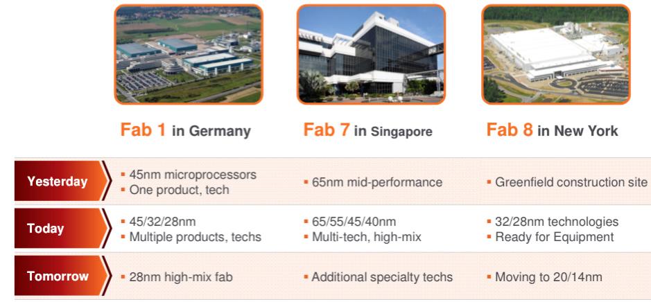 The capacity they have in place is quite impressive. Fab 1 (the old AMD fab in Dresden) is expanding to 80,000 wafer starts per month. I assume that means 300mm wafers rather than 200mm wafer-equivalents that is sometimes used. The focus is 45/40/32/28nm. Fab 8 (under construction in New York) is big: 6 football fields of clean room with over 7 miles of overhead track for moving wafer transport vehicles around. It will have 60,000 wafer starts per month once ramped, focused on 28/20nm. And in Singapore (the old Chartered fabs) they have a lot of 200mm capacity and, in fab 7, 50,000 wafer starts per month anywhere from 130nm to 40nm.
The meat of what Global is up to was in Gregg Bartlett’s presentation on the implementation of their process roadmap. He is very proud that they have gate-first 32nm HKMG ramped while other people using it are struggling. During the lunch he was asked about Intel’s 3D transistor. He thinks that despite some advantages, they will prove very difficult to control in the vertical dimension and are too restrictive for a general foundry business. Which is interesting if true since Intel has more capacity than it needs and so is entering the foundry business!
At 28nm they will use basically the same FEOL (front end of line, i.e. transistors) as at 32nm, namely gate-first HKMG. Compared to 40nm this is a 100% density increase and either a 40% increase in performance or a 40% reduction in power (depending on how you take it). He reckons that die are 10-20% smaller relative to 28nm gate-last processes. That would be TSMC.
But apparently at 20nm, litho restrictions mean that you can no longer get that 10-20% benefit so they will switch to gate-last. Versus 28nm this is nearly a 50% area shrink and they are investing in innovation in interconnect technologies.
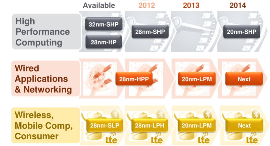 And after that? 16/14nm. Multi-gate FinFET transistors, lots of innovation. Also innovation in EUV (extreme ultraviolet) where they have been doing lots of development work (over 60 masks delivered) and will have production installation in New York in the second half of next year.


The Packaging PDK Is the Missing Layer for Co-Packaged Optics