wide 1

Critical Area Analysis and Memory Redundancy

Critical Area Analysis and Memory Redundancy
by SStalnaker on 10-08-2010 at 8:08 pm

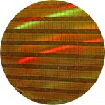
Simon Favre, one of our Calibre Technical Marketing Engineers, presented a paper on Critical Area Analysis and Memory Redundancy at the 2010 IEEE North Atlantic Test Workshop in Hopewell Junction, NY, just up the road from Fishkill. As Simon says…

Fishkill, New York. IBM is in Fishkill. IBM invented Critical Area Analysis in what, the 1960’s? Venturing into IBM country to speak on CAA is kind of like being the court jester. Fortunately, no one said, “Off with his head.” 🙂 But seriously, it amazes me how little is known about this topic.
Continue reading “Critical Area Analysis and Memory Redundancy”


Semiconductor Forecast 2010-2011 Update!

Semiconductor Forecast 2010-2011 Update!
by Daniel Nenni on 10-03-2010 at 10:35 pm

It’s that time of the quarter again, where the semiconductor analysts revise forecasts, passing off glorified guesstimates as valid financial planning data. They aren’t forecasts! They are observations! I blame these hacks for the 12.5% Silicon Valley unemployment rate! I blame these hacks for the dwindling available capitol for emerging fabless, EDA, and IP companies. I even blame these hacks for global warming! Okay, maybe not global warming, but the other stuff for sure!

iSupply is first out of the gate with a downward observation (forecast) of 32% versus 35%. Semiconductor revenues around the world are now expected to hit $302 billion this year, a gain of 32 percent from $228 billion in 2009. This drop is attributed to “weaker consumer demand for certain electronic devices and higher industry inventory” rather than “just bad forecasting”. Revenue in the fourth quarter is expected to drop by 0.3 percent, which will be the first sequential drop since the semiconductor market took an “unforecasted” nose dive in the fourth quarter of 2008 and first quarter of 2009.
TheSemiconductor Intelligence observation (forecast) was 36% so expect a revision from Bill Jewell. Bill also warns us that, according to National Bureau of Economic Research (NBER), the current recession is the longest since World War II:

The NBER is generally seen as the authority for documenting US recessions and defines them as:
“a significant decline in the economic activity spread across the country, lasting more than a few months, normally visible in real GDP growth, real personal income, employment (non-farm payrolls), industrial production, and wholesale-retail sales.”

By definition, the end of a recession means the U.S. economy stopped contracting and not when it reaches the level it was at the start, so we have a way to go yet. The US Real GDP & Durable Goods graphic is based on data from the U.S. Department of Commerce and shows the quarterly U.S. real gross domestic product (GDP) indexed to 4th quarter 2007, the peak prior to the recession.

Speaking of the semiconductor ecosystem, next week I will be at the 2010 TSMC OIP Partner Forum on Tuesday and the SMIC 2010 Technology Symposium on Friday, two free lunches, the life of a world famous blogger! It would be a pleasure to meet you, that is, of course, if you recognize me without the Porsche hat!


TSMC GigaFab Tour!

TSMC GigaFab Tour!
by Daniel Nenni on 10-01-2010 at 9:44 am

During my most recent Taiwan trip I was not only afforded a meeting with Dr Mark Liu, Sr VP of TSMC, a guided tour of GigaFab #12 was also included. Even more impressive, I’m now considered “Elite” by Eva Airlines so I automatically get the good seats, better food, and VIP service. My wife, however, is not impressed with my Elite status so I still have to do chores around the house.

Mark Liu ramped up TSMC’s first 200mm fab in 1993 and has been building fabs for TSMC ever since. Mark’s favorite topic is the 300mm GigaFabs, Fab#12, Fab#14, and Fab #15 which TSMC just broke ground on last month. Clearly TSMC has learned a valuable lesson from the 40nm wafer shortage experience. Not having enough capacity is far more costly than having too much. After 40nm, customer priorities have certainly changed: Capacity is now the 1st concern with price a close 2[SUP]nd[/SUP], and last but not least design enablement. Please note that the perceived value of semiconductor design enablement is often overlooked but it is clearly the key enabler to TSMC’s expansive customer base.
After putting on the clean room space suit and being lightly air washed I entered a GigaFab for the first time and was literally speechless. If you know me personally, being speechless is not one of my strong suits so this was a new experience.

The insignias on the machines were logos and acronyms that I recognized but what struck me was the total automation of a GigaFab. Machines outnumbered man exponentially with 99% automation. Shuttles zoomed around on tracks above delivering thousands of 40nm wafers to the 300+ steps in the semiconductor manufacturing process. The few people I did see were at monitoring stations. Even more impressive than the billions of dollars of hardware in a GigaFab, is the millions of lines of software developed to run it: Automated Material Handling Systems (AMHS) for transporting, storing, and managing semiconductor wafer carriers and reticles plus Manufacturing Execution Systems (MES) software to manage overall production efficiency.

This year TSMC will spend a record $5.9B on capital expenditures. Approximately 75% will be used to expand TSMC’s 65/40/28nm technology capacity and 15% will be used for mainstream processes. The remainder will be used for equipment, R&D expenses, and new business such as solar and LED. TSMC’s newest Gigafab, Fab 15, will cost an estimated $9.4B. TSMC is also set to complete Phase 5 expansion at Fab 12, and Phase 4 expansion at Fab 14.

According to the most recent management report, TSMC has accelerated its capacity expansion plan for 2010. Total managed capacity was 2,749K 8-inch equivalent wafers in 2Q10, increased by 7% from 2,566K in 1Q10. Current capacity plan calls for an overall increase by 14% to 11,299 8- inch equivalent wafers, compared with 11,247 8-inch equivalent wafers planned in the last quarter.

Demand for TSMC’s advanced technology wafers in all major semiconductor market segments again increased quarter to quarter. Among the advanced technologies, 40nm not only increased an additional 2% of TSMC’s revenue share, the output of Gigafab wafers processed using 40nm technology increased by 30% sequentially.

The 40nm race is officially over, TSMC wins by a landslide in regards to capacity, price, and design enablement. The race for 28nm dominance however is still on between TSMC, Samsung, and GlobalFoundries. Samsung is in production at 32nm so moving to 28nm should just be a process shrink. For TSMC and GlobalFoundries, 28nm is a completely new node which will bring new technical challenges. Still, in my opinion, the foundry race to 28nm is too close to call today and it will certainly be an exciting finish!


Semiconductor Realization!

Semiconductor Realization!
by Daniel Nenni on 09-20-2010 at 1:15 pm

Insanity is doing the same thing over and over again and expecting different results (Albert Einstein). Given that statement, according to John Bruggeman (Cadence CMO and EDA360 Chief Anarchist) the semiconductor industry is INSANE!

This year the EDA Tech Forum and the Global Semiconductor Alliance Expo were not only on the same day, but also at the same location, which saved me a trip to the Santa Clara Convention Center but the conference session overlap was INSANE!

The award for the best panel definitely goes to the GSA: From MIDs to Base Stations – Where Mobility Infrastructure Meets Innovation, featuring heavy weight semiconductor executives from fabless companies around the world: Scintera, NetLogic, PicoChip, Altera, and eSilicon. The fifth panelist was John Bruggeman!?!? Whoever put John B. on this panel is INSANE!

First let’s look at the semiconductor problem statement best illustrated by Aart Degues, Synopsys CEO, in last week’s blog:

It’s an INSANE attempt at bottom-up design where you try to find a vegetarian restaurant while avoiding your level 12 vegan mother in-law (been there, done that). It’s a complicated and somewhat treacherous trip through System, SoC, and Silicon design and implementation. Unfortunately, this trip is getting longer and more expensive every day which has officially qualified semiconductor design starts and fabless semiconductor start-ups as endangered species.

Enter EDA360. I now consider myself an EDA360 expert since I have read the vision statement 360 times, blogged about it: EDA360 Manifesto, EDA360 Redux, TSMC OIP vs CDNS OIP, and have had endless conversations with the foundries, fabless, EDA and IP companies alike. So far, EDA360 is all about the WHY, which is something I see everyday in working with the top semiconductor companies and foundries on leading edge technologies. I also now work with an Eastern European investment fund targeted at fabless semiconductor companies in Silicon Valley which may sound INSANE but I can assure you it’s not. There is still plenty of money to be made IF you can get an SoC into production on time and within a REASONABLE amount of money.

Per JohnB: EDA360 is a top down approach starting with System Realization – to SoC Realization – ending with Silicon Realization. The WHY of EDA360 makes complete sense, great vision, I’m on board, I even have an EDA360 shirt. The question I have is: exactly HOW is this going to work?

During the GSA panel John B. spoke last and challenged the panel to turn it upside down, start at the top and be SYSTEM versus SILICON driven. The lack of meaningful discussion on the topic was disappointing. This was an infrastructure innovation panel, right? The panelists knew JohnB was on the panel, right? The crowd definitely wanted more EDA360 discussion but left empty headed!

IF EDA360 is a fantasy and the cost of semiconductor design continues to increase exponentially, where will the design starts come from? Where is the meaningful discussion within the top EDA vendors on this topic? When will there be a panel with Wally, Aart, and JohnB? I would even invite Rajeev! WE NEED DESIGN STARTS!

Insanity is doing the same thing over and over again and expecting different results (Albert Einstein). Given that statement, according to Daniel Nenni (World Famous Blogger) the Electronic Design Automation industry is INSANE!


GlobalFoundries Exposed, Part II!

GlobalFoundries Exposed, Part II!
by Daniel Nenni on 09-12-2010 at 10:02 pm

EDA CEO panels are usually rather dull but this one definitely held my interest. It was standing room only and I was surrounded by familiar faces from not only EDA and IP company executives, but also representatives from the top semiconductor companies around the world! The theme of course was collaboration, promoting the GFI “IDM-Like” business model for the merchant foundry business, but there were some surprises.

Doug Grose, GFI CEO, is an engaging speaker and has quite an impressive resume, with 25 years at IBM before joining AMD as senior vice president of technology development, manufacturing and supply chain. While I have not met Doug Grose yet (hint), the people who I know that have, confirm my first impression, that his leadership and technical skills are well suited to the competitive challenges GFI faces.

“AMD has put a number of the long-held assumptions about how to gain efficiency to question, and we’ve found some very interesting ways to approach the problem,” said Dr. Grose. “AMD is looking for ways to cut waste and drive value to our customers-it’s an approach based on Lean fundamentals.”

After the introduction by Doug Grose, Mojy Chian, GFI senior vice president of design enablement, was the first speaker. I know Mojy from Conexant years ago and the spin-out Mindspeed Technologies. I also worked with Mojy and his team at Altera. If you want to know how to yield at TSMC 40nm, talk to Mojy and his Altera design enablement team! Mojy credited the Chartered Semi foundry and AMD integrated device manufacturing experience for GFI’s vision of a new type of collaboration between partners and customers.

Synopsys CEO Aart DeGeus was the speaker that blew me away. Aart’s presentation compliments my blog Mobile 2Drive Semi 4Ever! Aart definitely gets social media, the mobile internet revolution, and how it will shape the semiconductor industry for years to come. I would also guess that Aart, like me, has teenage kids and a vegan mother in-law that he avoids. Aart correctly stated that social media IS collaboration and that we are raising a new generation of collaborators, so we had better be prepared to enable them, unlike my computer science undergraduate experience where collaboration was called cheating!

Aart also introduced the word systemic (yes I had to look it up) and a mathematical equation correction: Semiconductor design enablement results are not a SUM but a PRODUCT. As in, if anywhere in the semiconductor design and manufacturing equation there is a zero, the results will be a bad wafer, die, chip, or electronic device, which supports GFI’s vision for a new type of collaboration between partners and customers.

The other panel members had interesting stuff to say as well but I’m out of space. Joe Sawicki was very funny. I really like Joe but in my mind I was playing a game of “Where’s Wally?” This was a CEO panel so where was Wally Rhines? The CEO of ARM was also not there, Rajeev Madhavan, CEO of Magma, was not invited. Lip-Bu Tan, Cadence CEO was there but I would have preferred Cadence CMO John Bruggeman. Lip-Bu looked bored and only briefly mentioned EDA360. By definition, EDA360 is all about collaboration and should have been the centerpiece of the Cadence presentation. Just my opinion of course, but I am an internationally recognized industry blogger.


GlobalFoundries Exposed!

GlobalFoundries Exposed!
by Daniel Nenni on 09-06-2010 at 9:45 pm


The GlobalFoundries Technical Conference last week was one of the best I’ve seen. The theme of the conference was “GlobalFoundries is bringing the collaborative IDM semiconductor design and manufacturing culture to the merchant foundry business!”

“We ramped volume production at the 45/40nm node well ahead of all foundries and we are poised to maintain this leadership at 32/28nm, with plans to extend this to the 22/20nm node.”

Gregg Bartlett, Senior VP of technology and R&D, did one of the most complete technology reviews I have seen, in 28 minutes! I was even afforded time with Gregg for follow-up questions after his presentation (the benefits of being a world famous blogger!).

Thus far, GFI has executed an incredible marketing and PR campaign, taking full advantage of TSMC, UMC, and SMIC’s conservative culture. My first concern is can GFI implement technically, especially in regards to yield? My second concern is can GFI offer competitive pricing and capacity? As we all know in the wafer business, pricing and delivery trumps all.

The most significant announcement at the conference was a very aggressive 32nm/28nm and 22nm/20nm roadmap. So in addition to supporting multiple versions of 45nm SOI, 40nm CMOS, and 32nm SOI, GFI will beat TSMC to multiple versions of 28nm and 20nm?

The gate-first versus gate-last issue also came up. GFI claims that gate-first will offer a 15-20% die area advantage over gate-last. Gate-first will also allow existing design practices. During a discussion with Dr. S.Y. Chiang, the senior vice president at TSMC in charge of R&D, I was told that a gate-last approach with restricted design rules would yield much better. Dr. Chiang also predicted that 20nm will require the gate-last approach due to added complexities. I asked Gregg Bartlett twice what gate strategy GFI would use at 20nm and was unable to get a clear answer.

he other interesting announcement was the GFI 28nm AMS reference flow:

“GLOBALFOUNDRIES has joined with Cadence to deliver the major elements of the AMS production design flow in Q3, 2010, with all of the flow steps supported by the GLOBALFOUNDRIES PDK. The reference flow contains PCells that enable critical advanced features within Cadence Virtuoso custom design tools. The complete production-level AMS flow is expected to be released to customers in Q4 2010, with silicon validation scheduled for early 2011.”

Another interesting thing I learned at the conference was revenue. Being a private company has distinct advantages, such as no required financial disclosures, but the GFI CEO did mention revenue. The combined AMD and Chartered manufacturing operations did $2.5B in revenue last year. In 2010, Doug Grose estimated $4B, which would put GFI in contention for the #2 slot with UMC. Given the technology road map, IDM like collaboration, deep pockets, and aggressive marketing and PR, I would put GFI in contention for #1 with TSMC.


Cloud Computing = Darknet! BEWARE!

Cloud Computing = Darknet! BEWARE!
by Daniel Nenni on 07-25-2010 at 5:47 pm

Cloud computing will be the tragic end to the digital world as we once knew it. As we become more and more dependent on mobile internet devices we become less and less independent in life itself. Consider how much of your critical personal and professional information (digital capital) is stored via the internet and none of it is safe. With a quick series of keystrokes from anywhere in the world your digital capital can be altered or wiped clean leaving nothing but skin and bones.

If you haven’t read the “Daemon” and “Freedom” books by Daniel Suarez you should, if you dare to take a peek into what cloud computing has in store for us all. Daniel Suarez is an avid gamer and technology consultant to Fortune 1000 companies. He has designed and developed enterprise software for the defense, finance, and entertainment industries. The book name “Daemon” is quite clever. In technology, a daemon is a computer program that runs in the background and is not under the control of the user. In literature a daemon is a god, or a demon, or in this case both.

The book is centered on the death of Mathew Sobol, PhD, cofounder of CyberStorm Entertainment, a pioneer in online gaming. Upon his death, Sobol’s online games create an artificial inteligence based new world order “Darknet”, which is architected to take over the internet and everything connected to it for the greater good. The interface to Darket is a pair of virtual glasses that acts much like a smartphone does today. While the technology described in the books seem like fiction, most of it already exists and the rest certainly will. The technology speak is easy to follow for anyone who has a minimal understanding of computers and the internet, very little imagination is required.

The book’s premise is “knowledge is power” or more specifically “He who controls digital capital wins”. So you have to ask yourself, how long before just a handful of companies rule the earth (Apple, Google, Microsoft)? Look at the amount of data Google has access to:

  • Internet and corporate intranet data (Google search engine)
  • Personal and professional internet browsing (Chrome)
  • Mobile communications (Android OS)
  • Google Email-Voice-Talk
  • Google Earth-Maps-Travel
  • YouTube

And dozens of other Google products that can be used to collect and manipulate public and private data in order to spy on us and ultimately control the world.

Cloud Computing is rampant with security flaws and backdoors which could easily enable the destruction of a person, place, or thing. A company or brand name years in the making can be destroyed within a day. In the book, a frustrated Darknet member erases the liquid assets of a non Darknet member who cuts in line at Starbucks. Depending on my mood that day, I could easily do this.

It’s not like we have a choice in all this since Cloud Computing is now a modern convenience. We no longer have to store our most private information in files, boxes, or even on our own computer hard drives. It’s a digital world and we are digital girls. The question is, who can be trusted to secure Darknet (Cloud Computing)?


Taiwan Semiconductor Manufacturing Corporation (NYSE: TSM)

Taiwan Semiconductor Manufacturing Corporation (NYSE: TSM)
by Daniel Nenni on 07-11-2010 at 10:09 pm

After working with TSMC the past 10+ years the single most compelling question I have is why the stock (NYSE: TSM) is not at record highs. TSMC invented and continues to dominate the foundry business which is clearly the future of modern semiconductor design and manufacture. So why is this not a $20+ stock?!?!?

TSMC reports 36%+ net margins.
TSMC delivers a 24%+ return on equity.
TSMC just announced a 3.8% dividend.
TSMC carries $6B+ total cash.
TSMC has more capacity than its top rivals combined and a third Gigafab under construction.
TSMC has almost a 7X Market Cap margin between its closest rival UMC.
So why is TSM flatlining after yet another record setting month of sales?!?!?

One of my favorite stock crowdsourcing groups agrees that TSM is undervalued. Based on the aggregate intelligence of 165k+ investors participating in Motley Fool CAPS, TSMC has a 5 out of 5 star rating. A Motley Fool CAPS rating indicates a stock’s potential to outperform the S&P 500 as determined by the community. On CAPS, 99% of the 437 All-Star members who have rated Taiwan Semiconductor Manufacturing Corporation believe the stock will outperform the S&P 500 moving forward.

Just how strong is TSMC in the global semiconductor foundry business? Well, with 45%+ market share, TSMC is about three times as big as its closest competitor, #2 foundry UMC, and more than six times as big as the #4 China based foundry SMIC. Even with the overly documented 40nm yield ramping problems, TSMC is still in charge of that node with an estimated 80% market share. Today, the race for 28nm is on with production silicon due out in Q1 2011. TSMC? GlobalFoundries? Samsung? It’s a 3 horse race, expect a photo finish, the winner is the King of the Node!

TSMC is expected to finish 2010 at $12.5B.
TSMC serves the largest and most diverse customer base.
TSMC will spend a record $4.8B on capital expansion this year.
TSMC will be trying to recruit 5,000 new employees this year.
TSMC is investing heavily in LED and Solar thin film PV technologies.
TSMC is the favorite to win the 28nm node foundry race next year.
TSMC has a 5 star Motley Fool CAPS rating.

Out of control consumer spending will continue to drive foundry revenues to record highs. Semiconductor industry mystics see foundry revenue growing 30-40% in 2010 and 8-10% annually over the next 4 years. Meanwhile, in 2010 shares of TSM and UMC are down 12% and 21%, respectively. So tell me again why TSM is yet another under performing tech stock?!?!


The New Semiconductor Economy

The New Semiconductor Economy
by Daniel Nenni on 07-04-2010 at 1:29 pm

Bill Wiseman of McKinsey & Company presented “Waking up to the new normal, the world economy after the great recession” at a recent ITAC GSA Conference. Bill supports my previous semiconductor financial predictions in great and graphical detail.

In the United States: unemployment claims are up, home sales are down without government incentives, and manufacturing growth is stalling. New claims for unemployment benefits recently jumped to 1.3 million people without federal jobless benefits, and that number could grow to 3.3 million by the end of the July due to political infighting. In Europe there is a debt crisis, in China there is an economic bubble, and the “double dip recession” search string is climbing the charts on Google.

The question is: How can we reconcile a slow & shaky macroeconomic recovery with a semiconductor industry that looks like this?

  • Almost every semiconductor company has blown away earnings forecasts and topped revenue estimates in recent quarters.
  • Foundries are running at near (or over) 100% utilization, and capex budgets are going through the roof (TSMC @ $5B+?).
  • Parts shortages are keeping capital equipment suppliers from working through their backlogs as fast as they want to.
  • Labor shortages in Southern China are forcing longer hours and higher pay for assembly workers at ODMs.
  • US retailers are seeing double digit same store sales growth in PCs, single digit in TVs and mobile phones.
  • Christmas was off the charts, inventory days in the value chain are at historic norms.
  • Wafer starts placed at TSMC and UMC will grow as much as 20% from Q2 to Q3.

Overall, the chip industry is “still in the overheating [phase]”, TSMC CEO Morris Chang said. “I don’t think it is excessive, but I do expect the growth rate next year may not be as high as everybody hopes.”

What Does Double Dip Recession Mean? When gross domestic product (GDP) growth slides back to negative after a quarter or two of positive growth. A double-dip recession refers to a recession followed by a short-lived recovery, followed by another recession.

The fate of the US economy hinges on whether new jobs appear in the coming months. For perspective, the U.S. requires 125,000 jobs per monthjust to keep up with population growth. “We’re not headed there (recovery) fast enough for a lot of Americans,” President Obama said. “We’re not headed there fast enough for me, either.”Very good observation Mr President!
In a recent essay: How to Make an American Job Before It’s Too Late, Andy Grove champions the job creation engine that once powered America:

The first task is to rebuild our industrial commons. We should develop a system of financial incentives: Levy an extra tax on the product of offshored labor. (If the result is a trade war, treat it like other wars — fight to win.) Keep that money separate. Deposit it in the coffers of what we might call the Scaling Bank of theU.S.and make these sums available to companies that will scale their American operations. Such a system would be a daily reminder that while pursuing our company goals, all of us in business have a responsibility to maintain the industrial base on which we depend and the society whose adaptability — and stability — we may have taken for granted.

I’m with Andy on this one, which is why I champion emerging technology companies. But in order for start-ups to create jobs in America, they must be able to scale in a competitive manner, and that is where the U.S. government is failing us.

lang: en_US


Atrenta Semiconductor Design in 3D!

Atrenta Semiconductor Design in 3D!
by Daniel Nenni on 06-27-2010 at 7:04 pm

My vote for most compelling technology at #47DAC is 3D technology. No, I don’t mean Hollywood-style 3D, I’m talking about vertical stacked-die system on chip design. This design approach basically means putting different parts of the system on different silicon substrates, so you can use the right technology for each part, and then stack them vertically.

3D technology promises to reduce cost and improve performance. By putting different parts of the system on a slice of silicon from an optimized process, you don’t have to do things like shoe-horn mixed signal parts into advanced process nodes, which is very expensive and doesn’t really work that well for mixed signal anyway. Because the interconnect between the silicon slices is very short (due to the stacking), wiring delays are minimized and performance should be very good.

There was a lot of talk about 3D at #47DAC last week. Many EDA vendors are jumping on the bandwagon and announcing plans to support it. A session that stands out as one of the more realistic and informative events on the topic was put on by Atrenta, IMEC, AutoESL, and Qualcomm. Front-end design issues were discussed and a front-end flow was demonstrated.

Besides seeing real, working software and not just PowerPoint, this session got my attention because it pointed out how different 3D design will be. One of the main challenges with this technology is choices, too many choices. The demo drove this point home by running different options for a 3D design through a high-level synthesis and virtual prototyping flow. AutoESL provided the high-level synthesis and Atrenta provided the virtual prototyping. If a designer would like to consider 3 different micro-architectures (like loop-unrolling, pipelining or standard) and three different technology choices (like 90, 65 or 40nm), then there are nine possible ways to implement this part of the 3D design. But which one should you choose?

The demo showed how to implement the three different micro-architectures and three different technology nodes by using various synthesis directives for the AutoESL tool. You start with C code and end up with RTL during this part. The Atrenta prototyping tool then read in the nine options and created a physical virtual prototype for all of them, complete with routing congestion and timing data. If you look at the options this way, it starts to become clear which one to choose.

I can’t imagine having the time to go through a complete back-end flow to figure this out, so the front-end planning part seems pretty important for 3D design. Another challenge with 3D appears to be thermal and stress modeling. Stacking dies like this creates all kinds of stress and heat problems. IMEC showed an interface between Atrenta’s prototyping tool and compact thermal and stress models they developed. Very impressive!

By the time this session was over, my brain was hurting from all the degrees of freedom implied by 3D. It will be interesting to watch as 3D becomes real over the next couple of years. We’ll see who wins, but for now, IMEC, Qualcomm, Atrenta, and AutoESL seem to have a jump on some of the hard problems. Please let me know your thoughts in the comment section, I can assure you, 3D EDA vendors will be reading them.