How could I talk about the various Interface protocols (PCIe, USB, MIPI, DDRn…) from an IP perspective and miss the PHY IP! Especially these days, where the PHY IP market has been seriously shaken, as we will see in this post, and will probably continue to be shaken… but we will have to wait and look at the M&A news during the next few weeks or so.
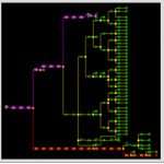
Before looking at these business related movements, doing some quick evangelization about what exactly is a PHY. The acronym comes from “PHYsical Media Attachment” (PMA) which described the part of the function dealing with the “medium” (PCB or optical). As of today, the vast majority of the protocols define high speed differential serial signaling where the clock is “embedded” in the data, at the noticeable exception of DDRn protocol where the clock is sent in parallel with the (non differential and parallel) data signals. The first reaction when seeing the layout view of an IC including a PHY function is that it’s damn small! A nice picture is always more efficient that a long talk, so I suggest you to look at the figure below (please note that the chip itself is a mid size IC, in the 30-40 sq. mm range).
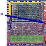
If we zoom in the PHY area, we will see three functional blocks: the PMA, usually mixed-signal, the Physical Coding Subsystem (PCS), pure digital as well as the block interfacing with the controller, named PIPE for Physical Interface for PCI Express in the PCI Express specification, SAPIS for SATA PHY Interface Specification and so on for the various specifications. Whatever the name, the functionality is always the same, allowing to interface high speed, mixed-signal and digital functions usually located in the pad ring (PMA and PCS) with the functional part of the specification (Controller) always digital and located into the IC core. The picture below shows a layout view for a x4 PCIe PHY. The Clock Management Unit (CMU) is a specific arrangement where the PLL and Clock generation blocks are shared by the four lanes.
Zooming again within the above picture, we would come to the PLL and the SerDes, both functions representing the heart of the PHY, requiring the most advanced know how to be designed. When sending data from the chip, you receive digital information from the controller, say a byte (parallel), then encode it (add 2 bits for encryption purpose) and “serialized” it to send 10 serial bits; this in case of 8B/10B encoding, valid for SATA or PCIe gen-1 or gen-2. For PCIe gen-3, encryption becomes 134B/136B when for 10 Gigabit Ethernet it’s 64B/66B. Precisely describing the various mechanisms used to build the different SerDes would take pages. Which is important to note here is that both the PLL and the SerDes design are requiring high level know how, and that Moore law allow to design faster and faster SerDes (but not smaller): in 2005, designing a 2.5 Gbit/s SerDes on a 90 nm technology what state of the art, now we are talking about 12.5 Gbit/s PHY designed on 28nm; and the 25 Gbit/s PHY able to support 100 Gigabit Ethernet using four lanes only (instead of ten 10G today) is not that far!
If we look at the business side, it’s easy now to understand that only a few teams around the world are able to design PHY functions, and an ever smaller number of companies to sell advanced PHY IP functions. Not because the market is small, in fact the massive move from parallel to serial interface specification has created a very healthy Interface IP segment weighting more than $300M in 2011, see this blog, but because it requires highly specialized design engineers, the type of engineers starting to do a decent job after five or ten years of practice, and being good after fifteen or twenty years experience!
Until very recently, end of 2011, the PHY IP vendor landscape was made of a large EDA and IP vendor, Synopsys, selling PHY + Controller IP to the mainstream market, but not so comfortable with the most advanced PHY products like PCIe gen-3 (8G) or 10 Gigabit Ethernet, competing with a couple of companies: Snowbush (IP Division of Gennum), MoSys (after the acquisition of Prism Circuit in 2009) and V Semiconductor, founded in 2008 by former Snowbush employees, as well as Analog Bits.
Snowbush, founded in 1998 by Pr Ken Martin (Professor of Microelectronic at Toronto University, this was the best location to hire young talents!), was considered by the market as the most advanced PHY IP vendor when the company was bought in 2007 by Gennum, a fabless company. Gennum realized that they had acquired a nugget, and quickly developed sales based on existing port-folio. They also realized that they were missing controller IP to be in the position to offer an integrated solution, and bought Asic Architect in 2008 for a very low price. At the same time, they fired the founders, including Pr Ken Martin, and try to develop and sale integrated solution, competing with Synopsys. Although Snowbush’ revenues quickly moved at the $10-12M range in 2008 and 2009, the company was still at the same level of revenue in 2011, on a market which grew 40% on the same period… As a matter of fact, if the PHY IP was still competitive, the controller IP never reach the same level of market acceptance.
Prism circuit was founded in 2007 and could compete on the same market than Snowbush (most advanced PHY developed in the latest technology nodes). The company was already doing good with a $5-6M range revenue when it was bought (for $25M, more than Snowbush!) in 2009 by MoSys. The rational was for MoSys to use SerDes technology from Prism Circuit to build an innovative product, the Bandwidth Engine IC, moving to fabless positioning, but still selling PHY IP… As we will see in a minute, this strategy was not as fruitful as expected.
In fact, both companies had success on a niche, lucrative segment (very high speed PHY) when a new comer, V Semiconductor, was started in 2008 by former Snowbush employees. V Semi was able to catch a good market share, as their revenue (not publicly disclosed) could be estimated around $10M in 2011. Among other design-in, they have designed the multi standard SerDes on Intel 28nm technology for FPGA start-up. This type of sale represent is a multi million dollar deal. Not that bad for supposedly not enough efficient business development people!
Untill 2011, we had a large EDA and IP vendor, enjoying the larger market share, challenged by a few PHY IP vendors, so customers still had the choice, especially when needing above 10 G PHY solution designed in advanced technology node.
Then, at the end of 2011, Gennum was acquired by Semtech, another fabless. A month ago or so (March 2012), it was clear that Semtech decided to keep Snowbush PHY for their internal use, which is a good strategy as such IP can be used as strong differentiators. The result is: PHY IP Vendor minus one. Then, still in March, came the announcement that Synopsys (see 8K form) has acquired MoSys PHY IP unlimited license for a mere $4.2M (former Prism Circuit was bought for $25M in 2009), preventing MoSys to grant new license. The result is now: PHY IP Vendor minus two!
There is still one or two vendors (V Semi and Analog Bits), you’d say… But Analog Bits is more design service than pure IP vendor oriented, supporting various mixed-signal products, from SerDes to SRAM/TCAM passing through PLL. And, last but not least, the rumors about an acquisition of V Semi are multiplying, days after days. As I don’t want to relay an unverified rumor, I will not disclose the last company name I have heard, but such an acquisition would not go in favor of more competition on the PHY IP market…
By Eric Estevefrom IPnest