Bronco Webinar 800x100 1

Selecting Non Volatile Memory IP: dynamic programming from Novocell Semiconductor lead to a lower “Cost Of Ownership”

Selecting Non Volatile Memory IP: dynamic programming from Novocell Semiconductor lead to a lower “Cost Of Ownership”
by Eric Esteve on 06-19-2012 at 9:07 am

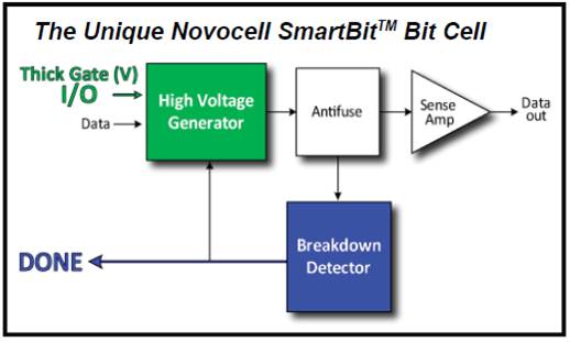
NVM IP offering from NovocellSemiconductor is based on SmartBit, an antifuse, One Time Programmable (OTP) technology, and the OTP block are embedded in standard Logic CMOS without any additional process or post process steps and can be programmed at the wafer level, in package, or in the field, as end user requires. What makes SmartBit technology unique is the “breakdown detector”, allowing to precisely determining when the voltage applied to the gate (allowing programming thememory cell by breaking the oxide and consequently allowing the current to flowthrough this oxide) will effectively have created an irreversible oxide breakdown, the “hard breakdown”, by opposition of a “soft breakdown” which is an apparent, reversible oxide breakdown. This is a first advantage: when the OTP programming step is completed, the user can be sure that every bit will have been set at the forecasted value. Apparently, this is not the case with each of the various OTP architectures, even if this is what you would naively expect from any NVM technology!

How do Novocell competitors proceed to program an OTP block, without this “breakdown detector” feature? They have to determine the“optimal programming timing” (the set time) provided to program each bit, which is determined for each specific foundry process (by technology node, and variation) and program the block according with this “set time”. Unfortunately, this ‘set time’ programming method will always result in some bits being ‘remnant’ bits un-programmed in the initial programming cycle. To be sure that every bit in the NVM block will have been set to the correct value, an additional programming cycle –at least- will be necessary to increase the yield. This approach is obviously time consuming (it takes at least twice the initial programming time), which can be pretty costly if, for example, you have to program the OTP using the tester, at wafer or packaged IC test step, when you consider the cost related to the test time on multi-million dollar devices. Another good point for SmartBit architecture: not only the programmingis more reliable, deterministic, but the cost of ownership linked to theprogramming step is cheaper.

Novocell competitors are trying to offer a safer approach, based on Error Correction circuitry or redundancy. Just take a look at what this precisely means, if we consider that some IP includes a full 2X redundancy of bits in order to achieve yield and performance requirements. Full redundancy can lead toeffectively doubling the area required on the chip for the customer-ordered bit density! A safer approach, even if it is theoretically not as safe as SmartBit, at the price of Silicon over cost. This over cost can be highly penalizing, when the NVM block is large and the device in production generating volumes that we see in the Consumer Electronic or Wireless Handset segments: million if not dozen of million units! Again, a costly tradeoff for an inferior programming methodology versus the Novocell dynamic approach based on “breakdown detection”…


Clearly, one of the Novocell’s differentiator is reliability, thanks to the “breakdown detector”. We also have seen that choosing SmartBit technology can dramatically reduce the total cost of ownership, by reducing programming time by a factor of 2 or more, and by using to a smaller NVM IP block size, leading to a smaller real estate or chip size than competitors, being forced to add redundancy to reach the same level of reliability – or yield.

Eric Estevefrom IPNEST –


What’s new with HSPICE at DAC?

What’s new with HSPICE at DAC?
by Daniel Payne on 06-18-2012 at 5:50 pm

One year ago I met with Hany Elhak of Synopsys to get an update on what was new with HSPICE in 2011, so this year at DAC Hany met me at the Synopsys booth for a quick update.

HSPICE has something called Precision Parallel so with 16 cores your IC circuit simulations will have about 10 x speed up compared to a single core.
Continue reading “What’s new with HSPICE at DAC?”


TSMC Threater Presentation: Solido Design Automation!

TSMC Threater Presentation: Solido Design Automation!
by Daniel Nenni on 06-17-2012 at 9:00 pm

For a small company, Solido has some very large customers and partners, TSMC being on of them. Why? Because of the high yield and memory performance demand on leading edge technologies, that’s why.

Much has been made of and will continue to be said on the march of Moore’s Law. While economics of scale and performance vs. power are the main justifications, there are increased design challenges that make designs of prior decades seem quaint by comparison. Smaller transistors allow for lower cost per function and more power efficiency, but they also come with increased variation effects, making performance vs. power vs. yield tradeoffs a necessary part of the design flow.

With each successive process shrink, there is a corresponding increase in the number of SPICE simulations required to push design performance while ensuring manufacturability. Solido Design Automation provides solutions for reducing the number of simulations needed during design and verification, while still providing the same or more visibility into design choices, impacts on yield and risk. As a leading provider of efficient variation analysis tools, Solido continues to collaborate with TSMC to deliver effective analysis capabilities on the latest nanometer technologies, supporting designers of memory, standard cell, low power, and analog/RF circuits.

Memory designers have perhaps the greatest challenge in maximizing their design performance within the capabilities of a particular process technology, needing to validate yield and performance to 4-6 sigma on bit cells and sense amps and 2-4 sigma at the array level. While Monte Carlo is the preferred solution, it’s simply impractical to simulate the billions of points needed for 6-sigma analysis. Since the analysis still has to be done, a number of approaches have evolved that seek to bypass Monte Carlo, but they each suffer limitations in accuracy, scalability and, especially, verifiability.

Solido’s Memory+ Suite goes back to the core Monte Carlo analysis designers trust and handles the billions of samples with intelligent adaptive techniques to focus simulation resources towards the high-sigma tails of the distribution. Since Memory+ uses actual Monte Carlo samples, it is able to provide simulation results around the target sigma, high-sigma corners for use in design development and even the full PDF. These options give designers the detailed insights they need into non-linear effects, design sensitivities to make informed sizing decisions.

Unlike other approaches, Solido’s Memory+ is able to handle the more severe non-linear responses, rendering it applicable to a broad range of memory cells. In the following example, a 3- or 4-sigma analysis would appear linear with extrapolation completely missing the failure regions occurring at +/- 4.5-sigma.

Additionally, with the full PDF available for both the bit cell and sense amp, Memory+ can provide 3-sigma analysis at the system level, allowing designers to explore performance vs. yield tradeoffs directly. The following table shows the results of a 3-sigma analysis on a 256Mb SRAM array using the Memory+ System Memory tool, enabling visibility into the tradeoff between timing and system-level yield, in a matter of minutes. The tool is also applicable to system-level DRAM analysis.

Using memory design as just one example, Solido is able to provide designers with the necessary tools to analyze yield and performance, faster and with more consistent quality than before. As shown with Memory+, memory designers can quickly analyze designs at the cell level to 6-sigma and the system-level to 3-sigma, while keeping Monte Carlo and SPICE level accuracy.


Cadence IP Strategy 2012

Cadence IP Strategy 2012
by Daniel Nenni on 06-17-2012 at 7:00 pm

As I mentioned in a previous blog Cadence Update 2012, Martin Lund is now in charge of the Cadence IP strategy. Martin read my first blog and wanted to exchange IP strategies so we met at DAC 2012 for a chat. Not only did Martin connect with me on LinkedIn, he also joined the SemiWiki LinkedIn group, which now has 4,000+ members. So yes, he is serious about social media and the IP business.

During his 12 years at Broadcom, Martin grew the company to become the global leader in Ethernet switch SoCs for data center, service provider, enterprise, and SMB markets, and successfully drove several strategic acquisitions. His silicon and system level experience equips him well to scale the Cadence SoC Realization business.

Prior to Broadcom, Lund held various marketing and senior engineering management positions in the Network Systems Division of Intel Corporation and at Case Technology, a European networking equipment manufacturer acquired by Intel in 1997. Lund is an inventor on 26 issued and pending US patents. He holds a technical degree from Frederiksberg Technical College and Risø National Laboratory at the Technical University of Denmark.

Being Danish, it should not have surprised me when Martin used the Lego analogy for IP. Lego is a Danish company and often compared to semiconductor IP as the building blocks of modern semiconductor design. Legos were my number one toy as a kid. My father was convinced I would be an architect, until of course I got my hands on a Comodore Pet computer, sorry about that Dad. Did you know that Lego is the largest tire manufacturer in the world? Martin did.

As a father of four, my Lego habit continued through my kids and Lego blocks evolved into Lego subsystems with optimized sets targeted at vertical markets. I remember spending hours with my son building a Space Shuttle kit and not one part was left over. A good analogy of the emerging semiconductor IP subsystems, plug and play, no parts left over.

What happened next to the space shuttle is the future of the IP business according to Martin Lund and I agree whole heartedly. My son made changes and incrementally optimized the shuttle for many different uses, until of course it was reduced to a pile of building blocks by his baby sister, and we were on to the next project which was even bigger, more complex, and in desperate need of optimizing.

Bottom line: For advanced semiconductor design, complete IP kits (off the shelf subsystems) will not work. There must be a significant level of optimization for differentiation and ease of integration. Trade-offs are an integral part of modern semiconductor design: Power, Performance, Area, Yield and IP subsystems will be held to the same standard. Off the shelf subsystems will not win in competitive markets. Mass customization will be required. Software will be the key enabler. Clearly this is a Cadence IP versus Synopsys IP strategy, which I will blog more about later.

Side note: My oldest son, the Lego Master, very quickly mastered the computer and internet. He is co-architect and lead administrator of SemiWiki and just received his Masters Degree in Education. Moving forward, he will prepare the legions of Lego Masters for the mathematical challenges of the new world order.


What Will Happen to Nokia?

What Will Happen to Nokia?
by Paul McLellan on 06-15-2012 at 3:06 pm

News today is that Moody’s has downgraded Nokia to junk status. They also announced that they will lay off 10,000 people (including about 1 in 4 of the people they employ in Finland, where Nokia is headquartered).

For those of you who don’t know all the inside-baseball stuff about Nokia, here is a recent little history. The current CEO of Nokia Stephen Elop came from Microsoft at the start of last year. He wrote a famous (infamous) memo known as the burning platforms (it started with the choice of people on burning oil platform to leap off). Since that memo sales have fallen for 5 consecutive quarters wiping out $13B in revenues and $4B in profits.

The first thing the memo did was to say that current products were not good and as a result people stopped buying them. This is known as the Rattner effect after a very profitable British jewellery chain called Rattners which had a store on every high street in Britain. At a dinner with finance types Gerald Rattner said that the stuff they sold was so cheap because it was “total crap.” It got into the press, people stopped going there and the chain quickly cratered in value and almost went bankrupt.

The next thing Elop did was decide that all smartphones would be based on Microsoft’s Windows Phone. This at a time when Nokia still dominated the smartphone market (outside the US) with phones based on Symbian and another internal operating system called Meego (despite the memo saying sales of Symbian-based smartphones were in terminal decline they were actually growing strongly and outselling Apple 2:1). The only problem was that these WP-based phones would not be available for the best part of a year. This is the Osborne effect, named after a silicon valley businessman (coincidentally also British) who announced that their next product would be compatible with the IBM PC. This was obviously desirable so everyone stopped buying the current products and the company ran out of money before it could deliver the sexy IBM-compatible one.


The effect of all of this is that Nokia has had the biggest loss of market share of any major business anywhere ever. By that measure Elop has to qualify as one of the worst CEOs of any company ever.

And worse, once the Lumia (WP-based) smartphone was available it didn’t sell very well. If you are going to put all your wood behind one arrow it had better be a good one and this one is not.

My go-to guy on anything to do with the phone market in general and Nokia in particular is Tomi Ahonen (who used to work at Nokia, is Finnish, but lives in Hong Kong these days). His view on what is going on are always worth reading. Cell-phones are not sold like other products (DVD players say). You can’t just go and buy any old cell phone and then go find a carrier (at least in most countries). The carriers control which phones get sold and which do not. Many cell-phone carriers also have landline businesses (often one cellphone license would go to the incumbent telecom operator in a country) and there is one thing that they absolutely hate: Skype. And who owns Skype? Microsoft. So the carriers hate Microsoft and aren’t going to do anything to help them. Hence the lukewarm launch of Lumia (on Easter Sunday when all the stores were closed, wonderful). Even Elop admits this saying that retail salespeople “are reticent to recommend Lumia smartphones to potential buyers.” So this hate goes all the way to the front lines.


So Nokia is in trouble, as I’ve said before. Of course they won’t go bankrupt and shut down, someone will buy them. So who? Tomi’s pick is Samsung although that was before the current round of layoffs and firings (he thinks they are damaged goods now). They are the only company other than Apple making any real money in handsets and would have huge market share, pick up some additional manufacturing lines in other parts of the world and so on. Microsoft could buy them but it would be easier for them to keep Nokia on life support by sending them money. Lots of people, in particular, Apple, could buy them for patents (although Nokia has been selling a lot of patents to keep afloat) and to stop Samsung getting them. Facebook could buy them if they really wanted to be in the handset business (but at lot of Nokia’s business is “feature phone” i.e. dumb phone). Lots of other choices of course. But this blog has gone on long enough.


TSMC Theater Presentation: Ciranova!

TSMC Theater Presentation: Ciranova!
by Daniel Nenni on 06-14-2012 at 9:00 pm

Ciranova presented a hierarchical custom layout flow used on several large advanced-node designs to reduce total layout time by about 50%. Ciranova itself does automated floorplanning and placement software with only limited routing; but since the first two constitute the majority of custom layout time, and strongly influence the remainder, the overall impact can be substantial. Designs sensitive to nanometer effects like Layout Dependent Effects (LDE) and poly density are particularly well suited to automation; one example was a 28nm, 40,000 device mixed-signal IP block which had been completely placed by one engineer in 8 days, including density optimization.

The Ciranova-enabled flow has two main phases. In the first phase, the software automatically generates a first-pass set of constraints for the entire design hierarchy, and a range of accurate floorplans. This phase is “push button” – it starts with a schematic and requires no intervention or user constraint entry. In the second phase, the user interactively refines the initial constraints, running and rerunning hierarchical placement until the entire layout matches the user’s floorplan targets and other criteria. The whole process is very fast; since the layouts are DRC-correct irrespective of rule complexity, tens of thousands of devices can be placed accurately in a few days. Ciranova’s output is an OpenAccess database which can be opened in any OA environment.

Two major advantages of this flow over normal schematic-driven-layout are (1) the DRC correct by construction aspect; and (2) the entire layout is optimized at once. This approach lends itself especially well to handling proximity-related effects like LDE, where the behavior of a given device changes depending on what happens to be nearby. Since Ciranova optimizes entire regions at once, multiple LDE spacing constraints are managed together.

In a TSMC design, TSMC provides tools at the schematic level to help a user identify LDE-sensitive devices in his or her schematic, and determine the relevant spacing constraints necessary for those devices to perform correctly. Ciranova then takes this information and produces a correct-by-construction layout which optimizes not only to the LDE directives but also to any other requirements: design rules, density, designer guidance such as symmetry, etc. Also, the approach is a general one and not limited to individual modules like current mirrors and differential pairs.

The diagram above includes a post-placement simulation study with alternate layouts of the same design: one with LDE rules applied, and one without (net result: the LDE-optimized placement clocks slightly faster). Most users never get to see a comparison like this, because hand layout takes so long that few people ever do it more than one way. But an automated flow makes this kind of study and tradeoff analysis easy.

Using this approach, even very large custom IC designs under very complex design rules can be done quickly; and typically at equal or better quality to handcraft, since much broader optimizations can be achieved than a human mask designer normally has time to explore.


Genevi, isn’t that a city in Switzerland?

Genevi, isn’t that a city in Switzerland?
by Paul McLellan on 06-14-2012 at 8:05 pm

I got an email from Mentor Embedded this morning about a webinar on Implementing a GENIVI-compliant System. I have to admit I had no idea what GENIVI is, which surprised me. I spent several years working in the embedded space and so I usually have at least a 50,000 foot view of most things going on there. One reason for my ignorance is that it only started in November 2011 unlike automotive standards such as FlexRay and CAN that have been around for a long time.

GENIVI turns out to be an automotive infotainment standard (the IVI on GENIVI stands for In-Vehicle Infotainment). This means it gets used in things like GPS maps, CD players, satellite access, but is not used for things like powertrain management or ABS braking (which are safety critical and so have a completely different set of tradeoffs). The GENIVI website describes itself as:”a non-profit industry alliance committed to driving the broad adoption of an In-Vehicle Infotainment (IVI) open-source development platform.”

GENIVI seems to be based in that hotbed of automotive…San Ramon, one valley over from Silicon Valley. Unlike, say, Android, Genivi is not an open-source development at the code level, it is a set of standard services, some of which are not optional, along with compliance programs.

The most recent specification of the specification is 2.0. On the prior iteration (that would be 1.0) 19 platforms from 9 member companies were declared compliant. Already under the 2.0 there are compliant platforms from:

  • Accenture
  • Intel/Samsung
  • Mentor Graphics (not exactly a surprise)
  • MontaVista
  • Renesas
  • Wind River

The obvious missing name is Google and Android.

The seminar will cover:

  • Implementing IVI, current trends and infrastructure
  • Gaining GENIVI compliance
  • Integrating open source and proprietary components
  • Building in adjacent functions, such as AutoSar and Android-based applications

The webinar is at 11am central time (9am on West Coast) on June 21st. Register for it here.


Semiconductor equipment returns to growth

Semiconductor equipment returns to growth
by Bill Jewell on 06-14-2012 at 7:37 pm

Semiconductor manufacturing equipment has returned to growth after a falloff in the second half of 2011. Combined data from SEMI (U.S. andEuropean companies) and SEAJ (Japanese companies) show billings peaked at a three-month-average of $3.2 billion in May 2011. Bookings and billings began todrop in June 2011, with billings reaching a low of $2.3 billion in November 2011. Bookings and billings began to turn around in December. Billings recovered to $2.9 billion in April 2012.


Total semiconductor manufacturing equipment billings were $33.4 billion in 2011. SEMI’s May 2012 forecast for wafer fab equipment called for 2% growth in 2012. 2% growth would result in $34.1 billion in billings for 2012, still 2% below 2007 billings of $34.7 billion and well below the record high of over $45 billion in 2000. Thus semiconductor capacity appears to be headed for moderate growth, but nowhere near the overheated growth which could lead to overcapacity.

What is the current capacity utilization in the semiconductor industry? The demise of the Semiconductor Industry Capacity Statistics (SICAS) program makes the answer difficult to determine. The final SICAS data for 4Q 2011 showed MOS IC capacity utilization of 88.9%, down from 91.7% in 3Q 2011. WSTS data showed a 2.3% decline in the semiconductor market in 1Q 2012 from 4Q 2012. Thus MOS IC shipments likely declined by a similar amount. MOS IC capacity growth was probably roughly flat in 1Q 2012 based on the falloff in manufacturing equipment billings in the second half of 2011. We at Semiconductor Intelligence estimate industry MOS IC capacity utilization was86% to 87% in 1Q 2012.

Forecasts for 2012 semiconductor market growth are generally fairly low. Mike Cowan’s June forecast was 0.3% growth, similar to WSTS’ May forecast of 0.4% growth. Our forecast at Semiconductor Intelligence is for 2% growth. Forecasts made in March and April from major semiconductor analyst firms range from 4% to 6%. Slow growth in the semiconductor market combined with slow growth in the semiconductor manufacturing equipment market should result in no significant movement in capacity utilization. MOS IC utilization should remain in the mid 80% range through 2012.

The two largest semiconductor foundries, TSMC and UMC, provide information on their wafer capacity and shipments. Data over the last year reflects the industry trends above. Both companies saw declines in revenue and shipments in 3Q 2011 and 4Q 2011. Shipments began to pick up in 1Q 2012. Both companies expect strong growth in business in 2Q 2012. TSMC expects 2Q 2012 revenue to increase 20% from 1Q 2012. UMC expects wafer shipment to increase 15%. Capacity growth has slowed significantly from prior quarters. TSMC expects capacity will decline 1.3% in 2Q 2012. UMC forecasts a 0.6% increase in capacity in 2Q 2012 following a 0.9% decline in 1Q 2012.