 RFIC developers used to favor mature silicon processes, typically staying back a couple of nodes behind the leading edge. This bought foundries time for ‘RF-enabling’ their PDKs, and also maximized return on investment for developing RF models and infrastructure IP. Not the case any more, it seems. To address the insatiable need for higher connectivity speeds and wider bandwidths, designers of SoCs with high performance gigabit/gigahertz transceivers will now opt for the latest process node, to benefit from higher transistor speeds and improved power/performance tradeoff. As a consequence, foundries and the IP/EDA ecosystem should now rush to RF-enable the leading process node, so that their customers can meet their time to market constraints.
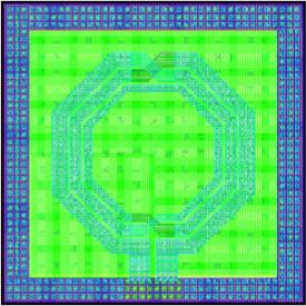
Backing this trend at 20 and 16nm, Helic recently released a library of resizable, parametric inductor cells that are fully lithography-compliant, meeting the restrictive design rules of these advanced nodes. The increased number of Design Rule Checks (DRCs) at the 20/16nm nodes, threatened to prohibitively increase the design effort needed for inductor design. Helic’s solution completely eliminates the need for tedious and time-consuming manual layout, by fully automating the process of layout creation according to designer specifications. The solution includes the automatic generation of dummy fill in the area taken up by a spiral, for meeting minimum density requirements in the fairly large areas taking up by inductors.
Helic’s parametric inductor cells can be used in a variety of 20/16nm IC and SoC designs, including wireless RF transceivers, multi-gigabit transceivers, frequency synthesizers and clock/data recovery circuits. The company aims to drastically shorten the design cycles of such products, which typically employ a good number of integrated inductors for increased performance (e.g. low clock jitter, wide amplifier bandwidth, etc.).
The library of 20/16nm inductors comprises a variety of spiral geometries, such as square and octagonal, including differential and transformer configurations. All these cells can be easily resized to meet a wide range of inductance, quality factor, operating bandwidth and current handling specifications. Helic also offers inductor compiler tools to further automate layout synthesis and optimization.
Helic will present its solutions for 20/16nm RF design, at the Design Automation Conference in Austin next week (booth no. 1843).
About Helic Helic, Inc.develops disruptive EDA technologies for RFIC and high-speed SoC design. We provide our customers with a comprehensive offering combining design tools, silicon IP and applications support, greatly reducing the development cycles of chips for wireless communications, broadband networking, PCs, tablets and other segments. We provide technology for rapid electromagnetics modeling, RF component synthesis, and signal integrity of silicon ICs and Systems-in-Package. Our solutions have been adopted by several major semiconductor companies since 2000. Helic is headquartered at 2880 Zanker road, Suite 203, San Jose, CA 95134.
Share this post via:


Chemical Origins of Environmental Modifications to MOR Lithographic Chemistry