At 28nm and below, a number of electrical variation effects become significant which depend not only on individual devices, but the physical interaction between neighboring devices, wells, etc during the manufacturing process. Some of these effects have become collectively referred to as “Layout Dependent Effects” (LDE); including the well-proximity effect, shallow trench isolation stress and a few others. Similar concerns include poly density, whose magnitude and variation can also affect device performance.
These effects are not easily predicted in circuit design, because they depend on detailed shape and layer interactions which don’t become known until the physical placement is complete. Yet they are also hard to manage in layout, because in any given context there are likely to be multiple interactions, and it’s often not obvious how they all net out electrically. Furthermore, EDA tool support to analyze LDE has so far been limited, and electrical performance data is really needed in circuit design, not layout.
The result is that while most advanced-node design groups are aware of LDE and other such context-sensitive effects, there are not currently well-accepted design flows to cope with them. Most 28/20nm groups today take one of two approaches, neither optimal:
[TABLE] align=”center” border=”1″
|-
| colspan=”2″ style=”width: 169px” | Current Approach
| style=”width: 186px” | Principle
| style=”width: 90px” | Advantages
| style=”width: 193px” | Disadvantages
|-
| style=”width: 22px” | 1
| style=”width: 147px” | Ignore LDE Altogether
| style=”width: 186px” | Assume the design is not critically sensitive to LDE
| style=”width: 90px” | Simple
| style=”width: 193px” | Risk: chip may yield poorly or even fail
|-
| style=”width: 22px” | 2
| style=”width: 147px” | Apply Conservative Rules to All Devices
| style=”width: 186px” | Increase die area until LDE effects are minimal on all devices
| style=”width: 90px” | Mitigates LDE
| style=”width: 193px” | Large area penalty since most devices not critical; may not solve Density issues
|-
What everybody would like is a “selective” LDE solution: a design flow in which the devices which really matter — those whose LDE-influenced behavior would materially impact the circuit’s performance — are identified early, and those devices and their surroundings are handled appropriately in layout; while the rest of the design is treated conventionally.
Unfortunately, this is difficult to implement within a traditional custom IC design flow, for several reasons:
- A standardized way to communicate LDE intent between circuit design, simulation and layout does not yet exist. If it’s done at all, it’s generally ad hoc.
- Laying out a region for LDE and Density is a complex optimization, with many potential interactions between devices, layers, wells, etc. And, it needs to be done in context of all the other nanometer design rules as well: grids, restricted pitches, poly rules etc. To do all this manually, with different rules for the same device in different contexts, is difficult and error-prone. Local changes as the layout and design rules evolve mean the optimization will likely be repeated multiple times. And a manual optimization is heavily dependent upon robust interactive LDE layout-vs-intent checking flows, which so far have not been widely available.
- Serious exploration at the physical level is essentially impossible, since traditional layout takes so long. No 28nm circuit designer gets to see his or her layout both with and without LDE optimization; there simply isn’t time to do two (or more) layouts.
As a result, robust and repeatable LDE optimization flows have yet to find their way into mainstream design. Standard 28/20nm practice today is either to risk LDE-related yield losses, or else to incur large area penalties.
A Simple LDE Optimization Flow
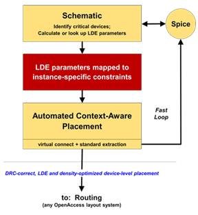
In order to address the 28/20nm LDE optimization problem, a practical and robust flow is needed that lets the circuit designer make design decisions which automatically propagate correctly through the rest of the implementation. We propose a simple flow, scalable to extremely advanced geometries, with four main elements:
[LIST=1]

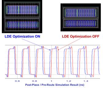
Below is a design constructed by a customer to pipeclean such a flow. It is a small, high-speed circuit. In this case two placements were done – in an automated flow it’s very easy to make multiple layouts. One layout has all devices set to “LDE-sensitive” and the other has all devices set “not LDE sensitive.”
The LDE conservatism used “default” data. The extraction was done with Mentor Calibre xRC and the simulation with Berkeley Design Automation’s Analog FastSPICE.

Three differences stand out. The first is the LDE-optimized design is faster. Not hugely so, but enough that you might well use it on a critical path, for example.
The second difference is that the LDE-compensated devices here took about 40% more area (and a manually optimized layout would likely be larger still). Fortunately in a larger design it’s unlikely the designers would want to apply LDE conservatism to more than a fraction of the devices in the design. If only 10% of the devices were designated “be careful with these, and their regions,” then the overall area penalty would be only a few percent, not 40%. A flow that can treat LDE selectively = good!
The third and possibly most interesting is that generating alternate tradeoff layouts with different combinations of devices designated “LDE on” and “LDE off,” or even LDE with more or less conservative parameters, is rapid and straightforward in this flow. Most circuit designers never get to see more than one layout for each circuit. Yet in environments where the layout has a material impact on the electrical performance, this kind of visibility can be immensely helpful.
Summary
As silicon geometries continue to shrink, designers can expect to see more and more sources of electrical variation which depend not just on individual devices, but on those devices’ proximity and relation to their surrounding context. Managing these designs will be greatly assisted by standardized methods of capturing LDE intent, and correct-by-construction layout which optimizes an entire device-level placement simultaneously for all nanometer silicon requirements at once; including LDE, Density, and future context-related concerns yet to be identified.
Eric Filseth,
Ciranova


Musk’s Orbital Compute Vision: TERAFAB and the End of the Terrestrial Data Center