You are currently viewing SemiWiki as a guest which gives you limited access to the site. To view blog comments and experience other SemiWiki features you must be a registered member. Registration is fast, simple, and absolutely free so please,
join our community today!
It feels to be at the top of semiconductor technology by having dies with high density of semiconductor design at sub-20nm technology node stacked together into a 3D-IC to form a complete SoC which can accommodate billions of gates. However there are multiple factors to be looked at in order to make that successful amid often conflicting… Read More
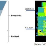
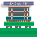
3D-IC has a stack of dies connected and packaged together, and therefore needs new testing strategies other than testing a single die. It’s given that a single defective die can render the whole of 3D-IC unusable, so each die in the stack must be completely and perfectly tested before its entry into that stack. Looking at it from a … Read More
At TSMC’s latest earnings call held mid January 2014, an analyst asked TSMC for a revenue forecast for their emerging 2.5/3D product line. C.C. Wei, President and Co-CEO answered: “800 Million Dollars in 2016 ”. TSMC has demonstrated great vision many times before. For me, an enthusiastic supporter of this technology, this statement… Read More
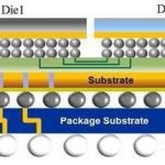
The first keynote at the Burlingame 3D conference was by Doug Yu of TSMC. Not surprisingly he was talking about 3D. In particular, TSMC has WLSI technology that they call CoWoS, which stands for chip-on-wafer-on-substrate which pretty much describes how it is built. This is the technology that Xilinx uses for its recently announced… Read More
AMD Goes 3Dby Paul McLellan on 12-13-2013 at 7:16 pmCategories: EDA
I attended the 3D packaging conference in Burlingame this week. The most interesting presentation to me was by Bryan Black of AMD. He argued very convincingly that Moore’s Law is basically over for the PC microprocessor business and the way forward is going to be 3D. AMD are clearly working on all this.
Increased density and… Read More
Two conferences on 3D, one just over and one coming up next week. The one that was just over was hosted by Georgia Tech, the 3rd Annual Global Interposer Technology Workshop (GIT). I wasn’t there but my ex-colleague from VLSI Technology Herb Reiter was. Herb has become very much associated with all things 3D since he led the … Read More
For the tenth year, the big 3DIC conference takes place in the Hyatt Regency at Burlingame (just south of San Francisco Airport). Officially it is 3D Architectures for Semiconductor Integration and Packaging or ASIP. This year there have already been some significant 3D announcements: TSMC’s 3D program, and Micron’s… Read More
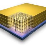
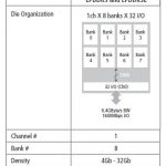
Today Micron announced that it is shipping 2GB Hybrid Memory Cube (HMC) samples. The HMC is actually 5 stacked die connected with through-silicon-vias (TSVs). The bottom die is a logic chip and is actually manufactured for Micron in an IBM 32nm process (and doesn’t have any TSVs). The other 4 die are 4Gb DRAM die manufactured… Read More
Lately I was studying about new innovations in memory world such as ReRAM and Memristor. As DRAM (although it has become a commodity) has found its extensive use in mobile, PC, tablet and so on, that was an inclination too to know more about. While reviewing Cadence’s offering in memory subsystems, I came across this whitepaperwhich… Read More
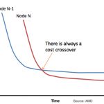
With the uncertainties around timing of 450mm wafers, EUV (whether it works at all and when) and new transistor architectures it is unclear whether Moore’s law as we know it is going to continue, and in particular whether the cost per transistor is going to remain economically attractive especially for consumer markets … Read More