You are currently viewing SemiWiki as a guest which gives you limited access to the site. To view blog comments and experience other SemiWiki features you must be a registered member. Registration is fast, simple, and absolutely free so please,
join our community today!
Next week it is Semicon West in the Moscone Center from Tuesday to Thursday, July 10-12th. Cadence will be on a panel session during a session entitled The 2.5D and 3D packaging landscape for 2015 and beyond. This starts with 3 short keynotes:
- 1.10pm to 1.25pm: Dr John Xie of Altera on Interposer integration through chip on wafer on
…
Read More
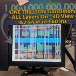
There are only a handful of billion transistor IC designs in existence today, so when an EDA company touts 1 trillion transistor IC layout editing then I take notice. This year at DAC I met with Katherine Hayes and Karen Mangum of Micro Magic to get an update on their IC layout tools.… Read More
EDPS: 3D ICs, part Iby Paul McLellan on 04-10-2012 at 10:00 pmCategories: EDA, Events
The second day (more like a half-day) of EDPS was devoted to 3D ICs. There was a lot of information, too much to summarize in a few hundred words. The keynote was by Riko Radojcic of Qualcomm, who has been a sort of one-man-band attempting to drive the EDA and manufacturing industries towards 3D. Of course it helps if you don’t … Read More
And no red and green glasses required.
I remember the first time I heard about a Through Silicon Via (TSV), punching a hole through the entire wafer to make an electrical connection at the back, like we do all the time in printed circuit boards with through plated holes. I thought someone was trying one on and trying to make me look a fool.… Read More
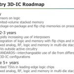
3D Standardsby Paul McLellan on 02-01-2012 at 5:06 pmCategories: Ansys, Inc., EDA
At DesignCon this week there was a panel on 3D standards organized by Si2. I also talked to Aveek Sarkar of Apache (a subsidiary of Ansys) who is one of the founding member companies of the Si2 Open3D Technical Advisory Board (TAB), along with Atrenta, Cadence, Fraunhofer Institute, Global Foundries, Intel, Invarian, Mentor, Qualcomm,… Read More
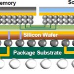
The ASIC business is getting more and more complicated. The ability to produce innovative die at a competitive price to solve increasingly complex problems just isn’t enough. The technology required to package that die is now front and center.
Here, at the junction of advanced design, process technology and state-of-the art … Read More
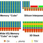
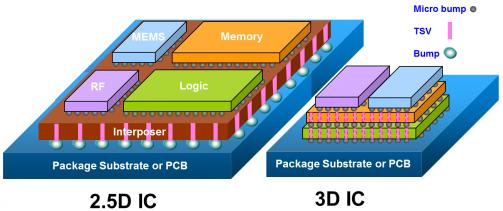
3D and 2.5D (silicon interposer) designs create new challenges for EDA. Not all of them are in the most obvious areas. Mentor has an interesting presentation on what is required for verification and testing of these types of designs. Obviously it is somewhat Mentor-centric but in laying out the challenges it is pretty much agnostic.… Read More