You are currently viewing SemiWiki as a guest which gives you limited access to the site. To view blog comments and experience other SemiWiki features you must be a registered member. Registration is fast, simple, and absolutely free so please,
join our community today!
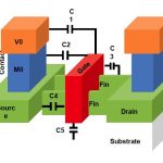
We read about FinFET technology in the semiconductor press daily now, thanks to Intel introducing their TriGate transistors starting in 2011 and creating a race with foundries and IDMs to switch from planar CMOS nodes. To get some perspective about the progress of FinFET IP and EDA tools I spoke with two experts from Synopsys, Swami… Read More
If you live in California anyway, with its large Asian population, you can’t have helped noticing that it was the Lunar New Year a couple of weeks ago, the start of the year of the sheep. A couple of days after the New Year, Xilinx announced their new families of what they now call FPGAs, 3D ICs and MPSoCs. But which the rest of us … Read More
For 20 years PDF Solutions have been working with fabs on yield enhancement. Today, they announced their Exensio Platform for big data manufacturing environments. They haven’t really been keeping it a secret and have been talking about it at events since late last year, but it has basically been in stealth mode for the last… Read More
IEDM 2014 was held in the second week of December 2014 in San Francisco. The excitement is over now and the dust has settled. Last week, at my leisure, I was glancing through the conference proceedings and short course material from IEDM 2014, when a slide from the 3DIC short course caught my attention. The slide presented below gives… Read More
Semiconductor business is highly dependent on technology and that changes very rapidly in the semiconductor space. It’s important to recognize the importance of research and innovation activities in this space. In my last article on 7nm technology node, one respondent commented, very rightly, “It’s important to have competition… Read More
- ASML making progress – but is it fast enough?
- ASML has missed 10nm , can it catch 7nm? An economic question
- Day one at SPIE- Better tone than last year but still cautious
1000 simulated wafers versus 700 simulated
At the opening of the SPIE conference ASML announced that TSMC had reached 1000 wafers a day “exposed”… Read More
‘Laughing Buddha’ is eternal, but for semiconductor industry, I must say it’s ‘laughing Moore’. Moore made a predictive hypothesis and the whole world is inclined to let that continue, eternally? When we were at 28nm, we weren’t hoping to go beyond 20/22nm; voices like ‘Moore’s law is dead’ started emerging. Today, we are already… Read More
Doing a modern SoC design is all about assembling IP and adding a small amount of unique IC design for differentiation (plus, usually, lots of software). If you re designing in a mature process then there is not a lot of difficulty finding IP for almost anything. But if you are designing in a process that has not yet reached high-volume… Read More
For about 5 years now Synopsys has held an HSPICE SIG event in conjunction with DesignCon. It features a small vendor faire with companies that partner with Synopsys on HSPICE flows. They also have a dinner with industry/customer speakers and provide an update on HSPICE development. Lastly there is a Q&A where customers get… Read More
One of the trending topics in Taiwan last week is the escalating conflict between Samsung and TSMC. This time however it is of a legal nature which has been a long time coming for the semiconductor industry. Reverse engineering has been an integral part of the semiconductor business since the beginning, as has intellectual property… Read More