You are currently viewing SemiWiki as a guest which gives you limited access to the site. To view blog comments and experience other SemiWiki features you must be a registered member. Registration is fast, simple, and absolutely free so please,
join our community today!
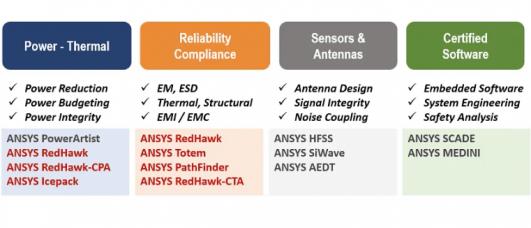
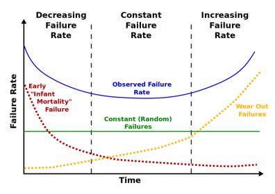
Ansys recently hosted a webinar on reliability signoff for FinFET-based designs, spanning thermal, EM, ESD, EMC and aging effects. I doubt you’re going to easily find a more comprehensive coverage of reliability impact and analysis solutions. If you care about reliability in FinFET designs, you might want to check out this webinar.… Read More
ANSYS and TSMC will be co-presenting at ARM TechCon on Multiphysics Reliability Signoff for Next Generation Automotive Electronics Systems. The event is on Thursday October 26th, 10:30am-11:20am in Grand Ballroom B.
You can get a free Expo pass which will give you access to this event HERE and see the session page for the event … Read More
Most people think that designing successful high speed analog circuits requires a mixture of magic, skill and lots of hard work. While this might be true, in reality it also requires a large dose of collaboration among each of the members of the design, tool and fabrication panoply. This point was recently made abundantly clear … Read More
Having followed GF since its inception, I agree with CTO Gary Patton, what we are seeing today truly is a different GLOBALFOUNDRIES! Our first GF blog was published on 9/13/2009 and we have done a total of 173 GF related blogs that have collected more than 1.5M views thus far. 72 of those blogs were written by me so I have followed this… Read More
Although the rejection of the Lattice deal was expected, it none the less has an impact on a number of dynamics in the chip industry and further M&A and consolidation. Freezing out China removes a “catalyst” in the market which help bid up values and add fear to both potential targets or those left out. Cross border… Read More
This year’s OIP was much more lighthearted than I remember which is understandable. TSMC is executing flawlessly, delivering new process technology every year. Last year’s opening speaker, David Keller, used the phrase “Celebrate the way we collaborate” which served as the theme for the conference. This year David’s… Read More
We are in the midst of a number of cross currents buffeting the industry. The Korea risk seems to have escalated again and our government has thrown fuel on the fire by threatening trade agreements at the most inopportune timing possible. However we are also a week away from the roll out of one of the most anticipated Iphones ever which… Read More
Being the number one EDA and the number one IP company does have its advantages and the resulting foundry relationships are a clear example. One of the DAC traditions that I truly enjoy is the Synopsys foundry breakfasts. Not only does Synopsys welcome scribes, they reserve a table up front for us and Synopsys CEO Aart de Geus has been… Read More
In 2014 Apple released the iPhone 6 which included the first SoC built on a TSMC (20nm) process. This phone started what many call a “Super Cycle” of people upgrading. According to Apple, they now have more than 1 billion activated devices so this super cycle could be seriously super, absolutely.… Read More
When someone says, “2.5D packaging” my first thought is TSMC and my second thought is Herb Reiter. Herb has more than 40 years of semiconductor experience and he has been a tireless promoter of 2.5D packaging for many years. Herb writes for and works with industry organizations on 2.5D work groups and events at conferences… Read More