You are currently viewing SemiWiki as a guest which gives you limited access to the site. To view blog comments and experience other SemiWiki features you must be a registered member. Registration is fast, simple, and absolutely free so please,
join our community today!
-Chips for America is better than nothing, but not much
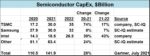
–TSMC $40-44B Capex crushes competition (Intel & Samsung)
-Additional efforts other than handouts are necessary
-Could/should TSMC be “adopted” as a US company?
Competition can’t keep up with $40-$44B of Capex
TSMC’s recent announcement… Read More
Previous SemiWiki articles have described the evolution of embedded non-volatile memory (eNVM) IP from (charge-based) eFlash technology to alternative (resistive) bitcell devices. (link, link)
The applications for eNVM are vast, and growing. For example, microcontrollers (MCUs) integrate non-volatile memory for … Read More
Advanced 2.5D/3D Packaging Roadmapby Tom Dillinger on 01-03-2022 at 6:00 amCategories: Events, Foundries, TSMC
Frequent SemiWiki readers are no doubt familiar with the advances in packaging technology introduced over the past decade. At the recent International Electron Devices Meeting (IEDM) in San Francisco, TSMC gave an insightful presentation sharing their vision for packaging roadmap goals and challenges, to address the growing… Read More
-Chips enable tech sector which underpins entire economy
-Is the US chip sector “Too Big To Fail”?
-If US chip industry fails, does tech & everything else follow?
-How chip/Taiwan crisis compares to 2008 financial meltdown
It was the best of times, it was the worst of times
We find it an incredible juxtaposition… Read More
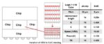
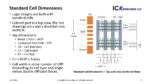
Standard Cell Scaling
Complex logic designs are built up from standard cells, in order to continue to scale logic we need to continually shrink the size of standard cells.
Figure 1 illustrates the dimensions of a standard cell.
Figure 1. Standard Cell Dimensions.
From figure 1 we can see that shrinking standard cell sizes requires… Read More
Dan is joined by Dr. Wally Rhines. Dan discusses the recent announcement that Wally is the newest recipient of the Dr. Morris Chang Exemplary Leadership Award. The meaning of the award and some history of Morris Chang and TSMC are discussed. The recent funding round for Cornami, led by SoftBank, is also discussed. What is Cornami… Read More
TSMC recently held their Open Innovation Platform (OIP) Ecosystem Forum event where many of their key partners presented on their latest projects and developments. This year one of their top IP provider partners, Analog Bits, gave two presentations. Analog building blocks have always been necessary as enabling technology … Read More
“Super” Moore’s Law- 5 nodes in 4 years- Too good to be true?
Gelsinger said “Intel will be advantaged with High NA EUV”
Ponte Vecchio better with “TSMC Inside”
Global Flounders IPO as price drops on public debut
Lets do the time warp again….(apologies to Riff Raff)
Its just … Read More
Semiconductor capital expenditures (CapEx) are on track for strong growth in 2021. For many companies the increase should continue into 2022. TSMC, the dominant foundry company, expects to spend $30 billion in CapEx in 2021, a 74% increase from 2020. TSMC announced in March it plans to invest $100 billion over the next three years,… Read More
The Apple event today was essentially a reveal of the latest and greatest silicon coming out of the Apple/TSMC partnership and how far ahead of everything else it is. The Mac was simply an aluminum container for the new silicon.
More importantly the event and specs of the TWO new chips, the M1 Pro and the M1 Max demonstrate that the M1… Read More