You are currently viewing SemiWiki as a guest which gives you limited access to the site. To view blog comments and experience other SemiWiki features you must be a registered member. Registration is fast, simple, and absolutely free so please,
join our community today!
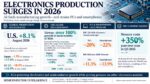
Growth in electronics production has been accelerating in 2026. Three-month-average change versus a year ago for electronics production in the U.S. was 8.1% in August 2026, continuing an accelerating growth trend since October 2025. Japan and the 27 countries of the European Union (EU 27) showed much stronger growth acceleration.… Read More
Applied Materials President and CEO Gary Dickerson with the EPIC Center founding partners on October 12, 2026, in Sunnyvale, CA. (Tomas Ovalle/AP Content Services for Applied Materials, Inc.)The bottlenecks are becoming interconnected
Artificial intelligence is changing what the semiconductor industry must deliver. … Read More
TSMC is describing an artificial intelligence boom that reaches beyond accelerator chips into the wider computing infrastructure needed to support increasingly capable AI systems. On the recent investor call, Chairman and CEO Dr. C.C. Wei presents strong demand, persistent supply constraints and an ambitious expansion … Read More
Sandra Rivera, Chair of VSORA, joined Bloomberg’s The Close in July for an interview on the current state of AI. What follows is a summary of that conversation.
When a Silicon Valley veteran who once ran Intel’s Data Center and AI Group, and now chairs a French inference-chip challenger, sits down with a tech journalist from Bloomberg,… Read More
TSMC’s 2026 Open Innovation Platform Forum presented artificial intelligence as the force reshaping semiconductor design. Its central argument is that faster chips will require progress across the whole system: logic, memory, packaging, interconnects, power delivery and design methods. TSMC places its partner ecosystem… Read More
Access to advanced semiconductor technology involves much more than choosing a process node. Design teams also need computing capacity, compatible tools, secure technology access, and experienced support. IC-Link by imec’s expanded collaboration with TSMC addresses that combination, potentially making sophisticated… Read More
One of the standout presentations at the 2026 TSMC OIP Forum highlighted a collaboration between Siemens EDA, Marvell, and TSMC. I always appreciate EDA presentations that bring together customer and foundry perspectives, and this one did not disappoint. We follow 3D IC technology closely and have published more than 150 blogs… Read More
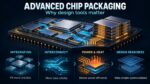
As chipmakers put more computing power into a single system, the challenge extends beyond making individual chips faster. They must connect multiple chips, memory stacks, power supplies, and sometimes optical components in a compact package. In the2026 TSMC OIP Forum talk “Addressing Inter-Die Complexity for 3D Multi-Die… Read More
Siemens and TSMC are expanding their collaboration on semiconductor design tools, with a focus on AI assisted workflows, advanced chip packaging and support for newer manufacturing processes. Their announcement centers on an AI agent intended to find and fix design rule violations: errors that can prevent a chip layout from… Read More
At the 2026 OIP Ecosystem Forum, the industry narrative shifted from incremental scaling to what TSMC defines as the “Intelligence Revolution.” Akin to the 18th-century Industrial Revolution which transitioned human physical labor to mechanical power, the current era is augmenting human ingenuity through … Read More