You are currently viewing SemiWiki as a guest which gives you limited access to the site. To view blog comments and experience other SemiWiki features you must be a registered member. Registration is fast, simple, and absolutely free so please,
join our community today!
For SoCs designed for various applications such as mobile, automotive, wearable computing, gaming, virtual reality, PC, imaging, security, and IOT applications, it is incredibly important to keep area (cost) and power as low as possible. Considering the growing percentage of chip area used for memory, it makes sense to choose… Read More
Two weeks ago I spoke on the phone with Albert Li, Founder and CEO of Platform DA about his EDA company. Prior to founding Platform DA in Beijing, Li worked at Accelicon which was acquired by Agilent in December 2011. Mr. Li graduated from Tsinghua University and Vanderbilt University, both in Electrical Engineering, and has written… Read More
I’ve done SRAM and DRAM design before as a circuit designer from 1978-1986, but in 2016 there are so many more challenges to using 28nm and 14nm on FDSOI technology. One way to keep abreast of SRAM design is to read conference papers, so I just finished a paper from authors at STMicroelectronics and MunEDA presented at the IEEE… Read More
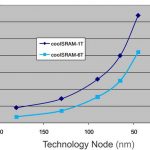
At ISSCC this year Samsung published a paper entitled “A 10nm FinFET 128Mb SRAM with Assist Adjustment System for Power, Performance, and Area Optimization. In the paper Samsung disclosed a high density 6T SRAM cell size of 0.040µm[SUP]2[/SUP]. I thought it would be interesting to take a look at how this cell size stacks … Read More
Recently Intel and Micron announced a new three dimensional cross point (3D Xpoint) memory. The 3D Xpoint announcement has generated a lot of questions and interest in what this new memory is and where it may fit in the semiconductor market. … Read More
SEMATECH, Silvaco and SRAMby admin on 09-04-2015 at 7:00 amCategories: EDA
SEMATECH has been around for over 20 years, starting in Austin. Today it is in upstate New York which increasingly seems to be the area for semiconductor research with IBM (still doing research although they sold their semiconductor business to GlobalFoundries), GlobalFoundries’ own Fab 8, the College of Nanoscale Science… Read More
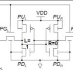
My IC design career started out with DRAM at Intel, and included SRAM embedded in GPUs, so I recall some common questions that face memory IP designers even today, like:
- Does reading a bit flip the stored data?
- Can I write both 0 and 1 into every cell?
- Will read access times be met?
- While lowering the supply voltage does the cell data retain?
…
Read More
Kilopass has a new VP of engineering, Jen-Tai Hsu. I sat down with him last week to find out where he came from and where he and Kilopass are going.
He grew up in Taiwan and went to National Taiwan University where he studied electrical engineering. Then he came to the US and went to Case Western Reserve University to get a masters degree,… Read More
Wearables and the Internet of Things (IoT) in general are all about low power. Everyone must have read (or even experienced) the phenomenon of putting something like a Fitbit on and then after a short period leaving it in a drawer or putting it to recharge and forgetting about it for weeks. The longer devices can last the more likely… Read More
In the beginning of this decade there was a lot of buzz around 3D chip manufacturing. Many EDA tools were developed to facilitate semiconductor designs in 3D space. Naturally, we are moving to the edge on 2D without much room to further squeeze transistors and interconnect. However, lately I haven’t heard much about 3D products.… Read More