Dan is joined by a panel of experts to discuss chiplets and 2.5/3D design. The panelists are: Saif Alam – Vice President of Engineering at Movellus Inc., Tony Mastroianni Siemens EDA- Advanced Packaging Solutions Director and Craig Bishop – CTO Deca Technologies.
In this spirited and informative discussion the … Read More
My recent article, ‘Chip War without Soldiers’ explained the importance of upskilling and preparing the chip design workforce in this current scenario, and it also explained how it will lead to ‘Fabs without Chips’ if we don’t prioritize it. VLSI Engineers are the pillars of the semiconductor industry, and they can only transform… Read More
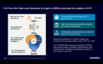
In the world of electronic systems design, complexity has always been a major challenge. As technology advances and demands for more efficient and powerful electronic devices grow, engineers face increasingly intricate design requirements. These complexities often lead to longer design cycles, increased costs, … Read More
Siemens EDA’s next move in its Calibre shift left strategy is the addition of correct-by-construction IC layout optimization for the most critical emerging physical design challenges. Calibre’s new DesignEnhancer product supports both custom and digital ICs and is already in use by several leading IC design companies. It … Read More
Next generation electronic systems require an engineering approach incorporating a digital twin methodology for early verification with digital prototypes. Over the course of a design project, the digital twin model evolves to allow more complex interactions including analysis, simulations and validations earlier… Read More
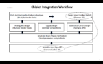
The transformation of the vertically integrated electronics value chain to a disaggregated supply chain has brought tremendous value to the electronics industry and benefits to the consumers. This transformation has driven the various players to become highly specialized in order to support the market trends and demands … Read More
Who first came up with this term shift-left ? I’d assumed Siemens EDA as they use it so widely. But their latest white paper on the productivity improvements possible with shift-left Calibre IC verification flows puts the record straight: a software engineer called Larry Smith bagged the naming rights in a 2001 paper (leapfrogging… Read More
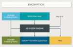
In the fast moving world of data communications, the appetite for high speed data transfers is accompanied by a growing need for data confidentiality and integrity. The wildly popular PCIe interface standard for connectivity has not only been increasing data transfer rates but has also introduced an Integrity and Data Encryption… Read More
It was refreshing to hear a talk focused on emerging stronger from the downturn when the news and media are focused on the gloom. At the recent Siemens EDA User2User conference, Joe Sawicki, executive vice president, IC, gave an uplifting keynote talk to the audience. He highlighted a secular growth trend happening in the semiconductor… Read More
Chiplet is a hot topic in the semiconductor world these days. So much so that if one hasn’t heard that term, the person must be living on a very isolated islet. Humor aside, products built using chiplets-based methodology have been in existence for at least some years now. Companies such as Intel, AMD, Apple and others have integrated… Read More