You are currently viewing SemiWiki as a guest which gives you limited access to the site. To view blog comments and experience other SemiWiki features you must be a registered member. Registration is fast, simple, and absolutely free so please,
join our community today!
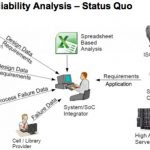
It has be come a cliche to say that “power is the new timing”, the thing that keeps designers up at night and drives the major architectural decisions in big SoCs. Nobody is saying it yet but perhaps “reliability is the new power” will be tomorrow’s received wisdom.
I talked to Adrian Evans of IROCTech… Read More
Moore’s Law has transcended computing expectations; however, its promise will eventually reach scalability limitations due to extraordinary consumer demands. Future technology encompasses breakthroughs capable of interaction with the outside world, which the More than Moore movement achieves. Through integrating … Read More
The fundamental economics of the semiconductor industry are summed up in the phrase “fill the fab.” Building a fab is a major investment. With a lifetime of just a few years, the costs of owning a fab are dominated by depreciation of the fixed capital assets (the building, the air and water purification equipment, the manufacturing… Read More
I used my secret powers (being a blogger will get you a press pass) to go to the first day of the SPIE conference on advanced lithography a couple of weeks ago. Everything that happens to with process nodes seems to be driven by lithography, and everything that happens in EDA is driven by semiconductor process. It is the place to find … Read More
During DVCon I met with Steve Bailey to get an update on Mentor’s verification. They were also announcing some new capabilities. I also attended Wally Rhines keynote (primarily about verification of course, since this was DVCon; I blogged about that here) and the Mentor lunch (it was pretty much Mentor all day for me) on the… Read More
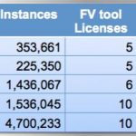
Formal verification can be used for many things, but one is to ensure that synthesis performs correctly and that the behavior of the output netlist is the same as the behavior of the input RTL. But designs are getting very large and formal verification is a complex tool to use, especially if the design is too large for the formal tool… Read More
Cavium designs some very complex SoCs containing multiple ARM or MIPS cores at 32 and 64 bit. This complexity leads to major challenges in validating the overall chip architecture to ensure that their designs will meet the requirements of their customers once they are completed, with performance as high as 100Gbps.
Cavium have… Read More
Almost no design these days is created from scratch. Typical designs can contain 500 or more IP blocks. But there is still a big difference between the first design for a new system or platform, and later designs which can be extensively based on the old design. These are known as derivatives and should be much easier to design since… Read More
Often as we move down the process node treadmill, new challenges appear that we didn’t really have to worry about before. Often, these challenges require addressing at a number of different levels: the process, the cell libraries, the design, the EDA tools that we use.
One well known example is the problem of metal migration.… Read More
Most mixed-signal design teams don’t use data management. Well, that’s not entirely true, everyone has to do data management of some sort, it is just that it is often very ad hoc, often done by some vaguely systematic way of doing file naming, using email to keep track of changes, no access control and so on. This leads… Read More