Back in the pre-SemiWiki days when I had the EdaGrafitti blog I wrote about the Carrington event. This was a solar storm in 1859 that lasted for several days. On September 1st there was a coronal mass ejection (CME) traveling directly towards earth. Normally such an event would take several days to reach earth but an earlier ejection… Read More
Tag: semiconductor
eSilicon and the Ten Minute Quote
One of the challenges in bringing a design into production is getting a quote that includes all the various stages of the process. The quote cycle typically takes a couple of weeks. It is also pretty wasteful. A typical design might be quoted by 3 manufacturers and so 2 out of 3 quotes are wasted expense because the design is lost to a … Read More
EUV Pellicles
Shakespeare reckoned that a man went through seven stages in his life.All the world’s a stage, And all the men and women merely players. They have their exits and their entrances, And one man in his time plays many parts, His acts being seven ages.
Well, an EUV mask seems to only go through three main stages:
[LIST=1]
Enterprise IP Management – A Whole New Gamut in Semiconductor Space
The world of IPs in the semiconductor landscape has completely changed the semiconductor design scenario, specifically the fabless design space. Today IPs are key components of any large semiconductor design, in the same way as auto ancillaries in auto design. It’s just the beginning, in the days to come we will see SoCs just as… Read More
Accelerating SoC Verification Through HLS
Once upon a time there was a struggle for verification completion of semiconductor designs at gate level. Today, beyond imagination, there is a struggle to verify a design with billions of gates at the RTL level which may never complete. The designs are large SoCs with complex architectures and several constraints of area, performance,… Read More
Taking a leap forward from TCAD
We all know that Technology Computer Aided Design (TCAD) simulations are essential in developing processes for semiconductor manufacturing. From the very nature of these simulations (involving physical structure and corresponding electrical characteristics of a transistor or device), they are predominantly finite-element… Read More
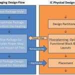
Temperature – The Fourth Aspect to Look at in SoC Design
In my career in semiconductor industry, I can recall, in the beginning there was emphasis on design completion with automation as fast as possible. The primary considerations were area and speed of completion of a semiconductor design. Today, with unprecedented increase in multiple functions on the same chip and density of the… Read More
Moderate growth and minor correction in semiconductors
At SEMICON West two weeks ago, Bob Johnson of Gartner presented the outlook for the semiconductor market, semiconductor capital spending, and wafer fab equipment spending. Thanks to Daniel Nenni for providing the link to the SEMI/Gartner Market Symposium presentations at https://sites.google.com/a/semi.org/market-symposium/home/speaker-presentations… Read More
When is a Million-Year MTBF Too Short?
The reliability metric, Mean Time Between Failures (MTBF), is often misunderstood. Use of an MTBF metric generally assumes a random failure process, one that is very infrequent and has no memory of past failures. Such failure modes can occur in System-on-Chip (SoC) designs and include radiation effects, synchronizer malfunctions… Read More
SEMICON Update: 450mm, EUV, FinFET, and More
I spent all of last week at SEMICON West meeting with customers, potential customers, partners and various industry analysts and experts. I was involved in many interesting discussions over the course of the week and I thought I would share some of the more interesting observations:
Alternate Fin Materials Pushed Out
I have for… Read More


