You are currently viewing SemiWiki as a guest which gives you limited access to the site. To view blog comments and experience other SemiWiki features you must be a registered member. Registration is fast, simple, and absolutely free so please,
join our community today!
This year’s Mentor Graphics user group meeting, User2User, will be held at the DoubleTree by Hilton in San Jose, California on April 25, 2013. The featured keynote presenters include…
- Dr. Walden C. Rhines, CEO and Chairman of Mentor Graphics, talking about “Organizing by Design”
- Victor Peng, Senior VP, Xilinx presenting on “The
…
Read More
My first job out of college was doing transistor-level circuit design, so I’m always curious about how companies are doing billion-transistor chip design and debug these days at the FPGA companies.
I spoke with Yaron Kretchmer,he works at Altera and manages the engineering infrastructure group where they have a compute… Read More
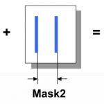
TSMC and Synopsys hosted a webinar in December on this topic of double patterning and how it impacts the IC extraction flow. The 20nm process node has IC layout geometries so closely spaced that the traditional optical-based lithography cannot be used, instead lower layers like Poly and Metal 1 require a new approach of using two… Read More
We will soon start to see the quarterly financial reporting installments of the “Big 3” public EDA companies. I predict they will be as boring as usual. I am not sure if I would want it any differently though.
Back in the 90s there were times when it was truly interesting to wait to see what Cadence, Mentor, or later Synopsys, might announce.… Read More
IC designers using advanced nodes are acutely aware of how variation effects in the silicon itself are causing increased analysis and design efforts in order to yield chips at acceptable levels. Four authors from Solidoare so passionate about this topic that they combined their years of experience into a book that I had a chance… Read More
D&R IP-SoC Days Santa Clara will be held on April 10, 2012 in Santa Clara, CA and if you plan to attend, just register here. IP market is a small world, and EDA a small market if you look at the generated revenue… but both are essential building blocks for the semiconductor industry. It was not clear back in 1995 that IP will become … Read More
Just because it seems that the likes given to: Interface Protocols, USB3, HDMI, MIPI… the winner and losers in 2011 were numerous, I decided to count it.
Twenty-four likes received, in 11 Linkedin groups (see below), that’s good! Very goos! Thanks to all of you… And most probably thanks to IPNESTfor the quality of the… Read More
Hardware designers use complex EDA tool flows that have collections of underlying binary and text files. Keeping track of the versions of your IC design can be a real issue when your projects use teams of engineers. ClioSoft has been offering HCM (Hardware Configuration Management) tools that work in the most popular flows of: … Read More
If you are doing transistor-level IC design then you’ve probably come up against questions like:
- What Changed in this schematic sheet?
- How did my IC layout change since last week?
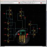
In the old days we would hold up the old and new versions of the schematics or IC layout and try to eye-ball what had changed. Now we have an automated… Read More
I met with Jeff Wilson, Product Marketing Manager at Mentor in the Calibre product group to learn more about Smart Fill versus Dummy Fill for DFM flows. Jeff works in the Wilsonville, Oregon office and we first meet at Silicon Compilers back in the 1990’s.
Dummy Fill
This diagram shows an IC layout layer on the left as originally… Read More


