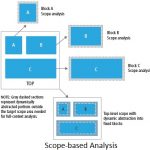
The semiconductor design sizes, these days, can easily be of the order of several hundred millions of cells, adding into the complexity of verification. Amid ever growing design sizes, it’s a must that the timing verification is done accurately. Normally Static Timing Analysis (STA) is done to check whether all clocks and signals… Read More
Tag: semiconductor design
Customization can add extraordinary power to your tool
In EDA arena we often find companies providing customization platforms along with the tools they offer to their customers. I admire such companies because they equip the end users of a tool to extend its functionality as they like according to their environment, thus increasing the designer productivity significantly. And I’m… Read More
Expert Constraint Management Leads to Productivity & Faster Convergence
The SoC designs of today are much more complex than ever in terms of number of clocks, IPs, levels of hierarchies, several modes of operations, different types of validations and checks for growing number of constraints at various stages in the design flow. As a semiconductor design evolves through several stages from RTL to layout,… Read More
IP Reuse and Management in Monterey!
One of the benefits of being part of SemiWiki is building relationships with a wide variety of companies covering every semiconductor design application imaginable. We are blessed, absolutely. Another benefit of being part of SemiWiki are the invitations to attend, participate, and even organize events such as EDPS. Last year… Read More
SEMulator3D 2014 – New Enhancements for Virtual Fabrication in the 3D IC Era
A Virtual Platform for any kind of design or manufacturing in any discipline of science or engineering (electrical, mechanical, aeronautics etc.) must be able to provide an accurate representation of an actual design/product in a fraction of time and cost it takes to build working prototypes. In the case of semiconductors at … Read More
IP Challenges, FinFET, 3D-IC, and FD-SOI Updates
Semiwiki is proud to be a sponsor of EDPS 2014:
April 17 & 18, 2014
Monterey Beach Hotel, Monterey, CA
Sponsored by:
IEEE Computer Society of Silicon Valley (CS-SCV)
IEEE Computer Society
Design Automation Technical Committee (DATC)
Council on Electronic Design Automation (CEDA)
The Electronic Design Processes Symposium… Read More
Evaluate MEMS Devices out-of-fab Before Fabrication
MEMS design and fabrication is highly complex in the sense that the fabrication process heavily depends on the design, unlike IC fabrication which has a standard set of processes. A slight change in MEMS design can alter its fabrication steps to a large extent. For example, setting device parameters such as capacitance or linear… Read More
Xilinx & Apache Team up for FPGA Reliability at 20nm
In this age of SoCs with hundreds of IPs from different sources integrated together and working at high operating frequencies, FPGA designers are hard pressed keeping up the chip reliability from issues arising out of excessive static & dynamic IR drop, power & ground noise, electro migration and so on. While the IPs are… Read More
Mark your Date for Semiconductor Design Vision
A very popular acronym is ‘WYSIWYG’ – What You See Is What You Get! This is very true and is important to visualize things to make it better in various aspects such as aesthetics, compactness, organization, structure, understandable for correction and so on; the most important, in case of semiconductor design, is being able to identify… Read More
A Tool Conceived With Designers’ Input and Developed from Scratch
If we look at the past, most of the EDA tools in the semiconductor design space have originated from a designers’ need to do things faster. Regardless of whether it is design exploration, manual design, simulation, verification, optimization (Power Performance Area – PPA) and many other steps in the overall design flow.… Read More


