You are currently viewing SemiWiki as a guest which gives you limited access to the site. To view blog comments and experience other SemiWiki features you must be a registered member. Registration is fast, simple, and absolutely free so please,
join our community today!
SEMICON is not just the event in San Francisco every July, there are other SEMICONs around the world. Coming up next, Shanghai China. In fact there are four colocated events:
- SEMICON China 2014, March 18th-20th
- The 8th PV fab managers’ forum, March 17th-18th (all things PhotoVoltaic)
- FPD China 2014, March 18th-20th (all
…
Read More
At the SEMI ISS conference earlier this week, the last speaker in the technology challenges section was Handel Jones of IBS. I’ve known Handel since the mid-1980s when he came to VLSI Technology and told us we were losing money on 90% of the designs we were doing but our cost model was not good enough and so we didn’t even… Read More
An Intel executive recently told me that my Intel articles on SemiWiki are used to motivate employees to work hard and prove me wrong. The converse is also true. The senseless Intel fabless ecosystem bashing motivates me to continue to write so it is a win-win scenario, absolutely. In fact, I should credit Intel’s Mark Bohr… Read More
The SEMI Industry Strategy Symposium (ISS) is Jan 13th-15th at the Ritz-Carlton in Half Moon Bay. When I discussed this with my beautiful wife as a possible business trip for us and mentioned the agenda she stopped me and said, “You had me at Ritz-Carlton!” As you can see by the picture it has a beautiful ocean view and includes a world… Read More
SEMI’s World Fab Forecast report, published in November, predicts that fab equipment spending will decline about -9 percent (US$32.5 billion) in 2013 (including new, used and in-house manufactured equipment). Setting aside the used 300mm equipment Globalfoundries acquired from Promos at the beginning of 2013 (NT$20-30 … Read More
I should start by saying that SEMI Smart Technology is not technology that is only half as smart as our phones, it is a conference on smart technology organized by SEMI. Officially it is called the International Technology Partners Conference with a sort of subtitle of From Smart Cars to Smart Cities: Shaping the Future of Microelectronics… Read More
With the uncertainties around timing of 450mm wafers, EUV (whether it works at all and when) and new transistor architectures it is unclear whether Moore’s law as we know it is going to continue, and in particular whether the cost per transistor is going to remain economically attractive especially for consumer markets … Read More
I attended the semi-annual SEMI Silicon Valley Lunch meeting last week. The semiconductor equipment people are the ones that really know what is going on. People can talk about capex numbers on conference calls but it is the equipment vendors who either do or do not get orders for particular types of equipment. In turn, the analysts… Read More
There are several events in Silicon Valley coming up of general interest to people working in EDA and the semiconductor industry.
SEMI 16th Annual Valley Lunch Forum. August 22nd, 11.30am to 1.30pm, Santa Clara Marriott
- What are the Opportunities for Advanced Semiconductor Devices?
- Where will the year end for 2013?
- Will we have
…
Read More
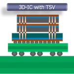
SEMICON Taiwan is September 3rd to 6th in TWTC Nangang Exhibition Hall. Just as with Semicon West in July in San Francisco, there is lots going on. But one special focus is 3D IC. There is a 3DIC and substrate pavilion on the exhibit floor and an Advanced Packaging Symposium. Design tools, manufacturing, packaging and testing solutions… Read More