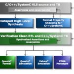
Of late, it has become painfully obvious that the value of electronics is in the system. And since systems demand continuing improvement, increasing performance and decreasing cost (once partially guaranteed by semiconductor process advances) is now sought through algorithm advances – witness the Google TPU and custom… Read More
Tag: mentor graphics
The Young and the Restless, PDA vs EDA, Photonic Soaps continued…
If you’ve followed my last article, The Guiding Light and Other Photonic Soaps, you read my comments about the use of waveguides to “guide the light” in photonic integrated circuits (PICs). This article continues the soap opera theme, this time with the Young and the Restless. My point here is that I am continually struck by the dichotomies… Read More
ARM sets up quagmire-free ecosystem for IoT
Wandering around DAC this week, I found much of the discussion focused on the EDA community being at an inflection point. How do we get more design starts from new places with new ideas without jeopardizing existing business? It’s not as simple a transition as it sounds.… Read More
Layout Pattern Matching for DRC, DFM, and Yield Improvement
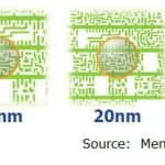
It is truly amazing to consider the advances in microelectronic process development, using 193i photolithography. The figure below is a stark reminder of the difference between the illuminating wavelength and the final imaged geometries. This technology evolution has been enabled by continued investment in mask data generation… Read More
What the #3 EDA company is showing at #53DAC this year
I live in Tualatin, Oregon just a few miles away from the corporate headquarters of the #3 EDA company in the world, Mentor Graphics. Since DAC is fast approaching, I thought it would be useful to give you a quick overview of what Mentor is going to be talking about in Austin, Texas during June 5-9. … Read More
Testing IGBTs before they go into EVs
In the pages of SemiWiki, we are usually talking about what to do with billions of really small transistors – for a change of pace today, we’ll discuss what to do with a few really big ones. Mentor Graphics has just announced their latest MicReD platform for thermal testing of IGBTs, experiencing a resurgence (pun intended) thanks… Read More
Army of Engineers on Site Only Masks Weakness
Hardware emulation was conceived in the 1980s to address a design verification crisis looming on the horizon. In those days, the largest digital designs were stressing the limits of the software-based, gate-level simulator that was the mainstream tool for the task.
It was anticipated and confirmed in short notice that adopting… Read More
Channel Operating Margin (COM) — A Standard for SI Analysis
There’s an old adage, attributed to renowned computer scientist Andrew Tannenbaum, one that perhaps only engineers find amusing: “The nice thing about standards is that you have so many to choose from.” Nevertheless, IEEE standards arise from customer requirements in the electronics industry. Many relate… Read More
Are Layoffs Good for the Semiconductor Industry?
As I have mentioned before, semiconductor professionals are very smart people, pound for pound the smartest in the workforce in my opinion. So what happens when thousands of engineers from Qualcomm, Broadcom, Altera, and Intel get shown the door? They don’t go to work for Starbucks, they don’t go to the unemployment line, they … Read More
Ecosystem Partnership for Effective Network Hardware Design
When you’re designing a hardware solution to plug into what is arguably the most complex system of all – the Internet – you can’t get away with a little fake traffic to test whether your box is going to do all the right things at the right performance. You have to model realistic voice, video, data and wireless traffic in… Read More


