You are currently viewing SemiWiki as a guest which gives you limited access to the site. To view blog comments and experience other SemiWiki features you must be a registered member. Registration is fast, simple, and absolutely free so please,
join our community today!
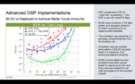
The need for speed is a never-ending story when it comes to data communications. Currently there are a number of trends such as cloud computing, artificial intelligence, Internet of Things (IoT), multimedia applications and consumer expectations driving this demand. All of these trends are accelerating the growth in high-performance-computing… Read More
I don’t know the story behind the name Alchip. I’ve been asking this question ever since its founding in 2003 and still haven’t found the answer. Wikipedia sometimes provides insights and stories behind names of companies, products and services but I couldn’t find any regarding the name Alchip. One thing is for sure. After its consistent… Read More
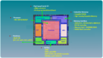
Successful ASIC providers offer top-notch infrastructure and methodologies that can accommodate varied demands from a multitude of customers. Such ASIC providers also need access to best-in-class IP portfolio, advanced packaging and test capabilities, and heterogeneous chiplet integration capability among other things.… Read More
According to the experts, the semiconductor industry is poised for a decade of growth and is projected to become a trillion dollar industry by 2030. In 2021 the semiconductor industry finally hit $600B so $1T by 2030 seems like a big ask, but not really if you look at the indicators inside the semiconductor ecosystem. Foundries, … Read More
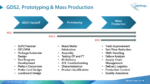
ASICs by definition are designed to meet the respective applications’ requirements. ASIC engineers deploy various design techniques to maximize performance, minimize power and reduce chip size. But is there more that can be done after the GDSII is taped out? A recent press release from Alchip Technology dated Feb 4, 2021 claims… Read More
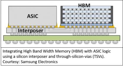
High Bandwidth Memory (HBM) systems have been successfully used for some time now in the network switching and high-performance computing (HPC) spaces. Now, adding fuel to the HBM fire, there is another market that shares similar system requirements as HPC and that is Artificial Intelligence (AI), especially AI systems doing… Read More
Until recently, ICs at bleeding edge nodes like 7nm technology from foundries like TSMC were mostly targeted for high-performance-computing (HPC) and mobile applications or possibly high radix switches that needed the increased performance of advanced nodes. The momentum of Moore’s law and Moore-than-Moore saw foundries… Read More
Open Silicon hosted a webinar today focusing on their High Bandwidth Memory (HBM) IP-subsystem product offering. Their IP-subsystem is based on the HBM2 standard and includes blocks for the memory controller, PHY and high-speed I/Os, all targeted to TSMC 16nm FF+ process. The IP-subsystem supports the full HBM2 standard with… Read More
Calling all ASIC designers working on High-Bandwidth Memory (HBM) access architectures in high-performance computing (HPC), networking, deep learning, virtual reality, gaming, cloud computing and data center applications. You won’t want to miss this upcoming webinar focused on system integration aspects of a HBM2 ASIC… Read More