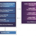
There is an emerging set of advanced packaging technologies that enables unique product designs, with the capability to integrate multiple die, from potentially heterogeneous technologies. These “system-in-package” (SiP) offerings provide architects with the opportunity to optimize product performance, power, cost,… Read More
Tag: hbm
Succeeding with 56G SerDes, HBM2, 2.5D and FinFET
eSilicon presented their advanced ASIC design capabilities at a seminar last Wednesday evening. This event was closed to the press, bloggers and analysts, but I managed to get some details from a friend who attended. The event title was: “Advanced ASICs for the Cloud-Computing Era: Succeeding with 56G SerDes, HBM2, 2.5D and FinFET… Read More
CEO Interview: Taher Madraswala of Open-Silicon
Taher Madraswala started his career at Intel designing microprocessors and later overseeing ASIC development before joining Open-Silicon at its inception. During his 25 year semiconductor career Taher has experienced more than 300 tapeouts across a wide variety of applications.
Today Open-Silicon applies an open business… Read More
Emergence of Segment-Specific DDRn Memory Controller
The semiconductor industry is served today by memory devices supporting various protocols, like DDR4, DDR3, LPDDR4, LPDDR3, GDDR5, HBM, HMC, etc. The trend is clearly to define application specific memory-protocols and in some cases, application specific devices. But developing many, and different, memory controllers … Read More
16nm HBM Implementation Presentation Highlights CoWoS During TSMC’s OIP
Once a year, during the TSMC’s Open Innovation Platform (OIP) Forum you can expect to see cutting edge technical achievements by TSMC and their partners. This year was no exception, with Open-Silicon presenting its accomplishments in implementing an HBM reference design in 16nm. It’s well understood that HBM offers huge benefits… Read More
10 signs on the neural-net-based ADAS road
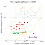
Every day I read stuff about the coming of fully autonomous vehicles, and it’s not every day we get a technologist’s view of the hurdles faced in getting there. Chris Rowen, CTO of Cadence’s IP group, gave one of the best presentations I’ve seen on ADAS technology and convolutional neural networks (CNNs) at #53DAC, pointing… Read More
Webinar alert – another break in the memory wall
A couple months ago we heard from another vendor in a webinar on HBM and breaking through the “memory wall”. Next week Open Silicon weighs in on the topic in a webinar with partners SK Hynix and Synopsys.… Read More
2.5D supply chain takes HBM over the wall
SoC designers have hit the memory wall head on. Although most SoCs address a relatively small memory capacity compared with PC and server chips, memory power consumption and bandwidth are struggling to keep up with processing and content expectations. A recent webinar looks at HBM as a possible solution.… Read More
Optimizing memory scheduling at integration-level
In our previous post on SoC memory resource planning, we shared 4 goals for a solution: optimize utilization and QoS, balance traffic across consumers and channels, eliminate performance loss from ordering dependencies, and analyze and understand tradeoffs. Let’s look at details on how Sonics is achieving this.… Read More
Bridging Design Environments for Advanced Multi-Die Package Verification
This year is shaping up to be an inflection point, when multi-die packaging technology will experience tremendous market growth. Advanced 2.5D/3D package offerings have been available for several years, utilizing a variety of technologies to serve as the package substrate, interposer material for embedding die micro-bump… Read More


