Last week I talked to Marco Brambilla of Synapse Design. Synapse is a design services company headquartered in Silicon Valley. It was founded in 2003 by Satish Bagalkotkar and has been profitable since the beginning. Today it has over 700 people. In addition to the headquarters in Santa Clara, they have a software group in Colorado,… Read More

Tag: finfet
Calibre xACT Shakes Up 16nm and Below Extraction Game
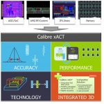
Mentor Graphics made a big announcement regarding SOC extraction at their User2User conference in San Jose during April. Before I get to the meat of the announcement, I’d like to reflect back on the early days of Calibre-DRC at Mentor. I was in Sales at Mentor around 1999, and Calibre-DRC was the new kid on the block. We had to go convince… Read More
PDK Generation Needs Paradigm Shift
For any semiconductor technology node to be adopted in actual semiconductor designs, the very first step is to have a Process Design Kit (PDK) developed for that particular technology node and qualified through several design tools used in the design flow. The development of PDK has not been easy; it’s a tedious, time consuming,… Read More
ANSYS Enters the League of 10nm Designs with TSMC
The way we are seeing technology progression these days is unprecedented. It’s just about six months ago, I had written about the intense collaboration between ANSYSand TSMCon the 16nm FinFET based design flow and TSMC certifying ANSYS tools for TSMC 16nm FF+ technology and also conferring ANSYS with “Partner of the Year” award.… Read More
SoCs in New Context Look beyond PPA
If we look back in the last century, performance and area were two main criteria for semiconductor chip design. All design tools and flows were concentrated towards optimizing those two aspects. As a result, density of chips started increasing and power became a critical factor. Now, Power, Performance and Area (PPA) are looked… Read More
FD-SOI Foundry
At the end of last month during ISSCC there was a forum organized by the SOI Consortium. It took place in San Francisco at the Palace Hotel (which, if you have never been there, is famous for converting its old entryway for carriages into an amazing dining room, and for a bar with a huge painting by Maxfield Parrish of the Pied Piper valued… Read More
FinFET Design Enablement
We read about FinFET technology in the semiconductor press daily now, thanks to Intel introducing their TriGate transistors starting in 2011 and creating a race with foundries and IDMs to switch from planar CMOS nodes. To get some perspective about the progress of FinFET IP and EDA tools I spoke with two experts from Synopsys, Swami… Read More
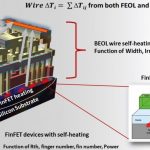
FinFET Designs Need Early Reliability Analysis
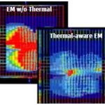
In a world with mobile and IoT devices driven by ultra-low power, high performance and small footprint transistors, FinFET based designs are ideal. FinFETs provide high current drive, low leakage and high device density. However, a FinFET transistor is more exposed to thermal issues, electro migration (EM), and electrostatic… Read More
7nm node is arriving, which ones will continue past 2020?
‘Laughing Buddha’ is eternal, but for semiconductor industry, I must say it’s ‘laughing Moore’. Moore made a predictive hypothesis and the whole world is inclined to let that continue, eternally? When we were at 28nm, we weren’t hoping to go beyond 20/22nm; voices like ‘Moore’s law is dead’ started emerging. Today, we are already… Read More
AMAT Earnings Call: Next Generation FinFETs?
The Applied Materials earnings call was last week. As usual I”m not all that interested in the financial details of the quarter and I’m certainly not the person to pick whether the stock is going to go up or down in the immediate future. However, there is always interesting information to be gleaned from the semiconductor… Read More