You are currently viewing SemiWiki as a guest which gives you limited access to the site. To view blog comments and experience other SemiWiki features you must be a registered member. Registration is fast, simple, and absolutely free so please,
join our community today!
Looking back, 2015 was a significant year for mergers and acquisitions in the EDA industry. The Semiwiki team maintains a chronology of major transactions here.
As I was reviewing this compendium, one of the entries that stands out is the acquisition of Apache Design Solutions by Ansys, Inc. a couple of years ago.
At that time, there… Read More
Often when a company starts out it takes a while for it to find the sweet spot in the marketplace. Very often it is feedback from existing customers and business success that can help point the way for small companies as they grow. This is just as true in EDA as it is in retailing or consumer products. For instance, Mentor Graphics, though… Read More
Often we hear about isolated instances of excellence from various companies in the semiconductor industry which contribute significantly in building the overall ecosystem. While the individual excellence is essential, it’s rather more important how that excellence is utilized in a larger way by the industry to create a ‘value… Read More
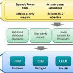
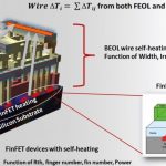
By the time that your SoC comes back from the fab and you plugin it into a socket on a board for testing, it’s a little late in the cycle to start thinking about reliability concerns like: dynamic voltage drop, noise coupling, EM (Electro-Migration), self-heating, thermal analysis and ESD (Electro-Static Discharge). They… Read More
The way we are seeing technology progression these days is unprecedented. It’s just about six months ago, I had written about the intense collaboration between ANSYSand TSMCon the 16nm FinFET based design flow and TSMC certifying ANSYS tools for TSMC 16nm FF+ technology and also conferring ANSYS with “Partner of the Year” award.… Read More
Silvaco Swallows Invarianby admin on 03-20-2015 at 7:00 amCategories: EDA
Yesterday, Silvaco announced that it has acquired Invarian Inc. Details of the transaction were not disclosed.
Who is Invarian? They are a recognized leader in block-level to full-chip sign-off analysis for complex, high-performance ICs. Their unique methodology utilizes a parallel architecture and concurrent power-voltage-thermal… Read More
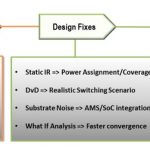
One of the big challenges in designing ICs today is designing a robust power net capable of delivering necessary current levels to all areas of the die. Getting it wrong can, of course, lead to circuit failures that range from non-functional silicon, through intermittent performance and functional problems, to early EM-driven… Read More
ANSYS makes a big deal of being a multi-physics company. Still it has taken them a while to fully integrate Apache. Nevertheless it seems like there is a compelling argument for combining technologies to solve SOC design problems. Frankly most chip designers would be hard pressed to think of a reason for using computational fluid… Read More
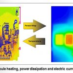
One of the big challenges in a modern SoC is doing an accurate analysis of the power nets. Different layers of metal have very different resistance characteristics (since they vary so much in width and height). Even vias can cause problems due to high resistance. Typically power is distributed globally on high-level metal layers,… Read More
I’ll never forget debugging my first DRAM chip at Intel, peering into a microscope and watching the aluminum interconnect actually bubble and dissolve as the voltage was increased, revealing the destructive effects of Electromigration (EM) failure. That was back in 1980 using 6 um, single level metal technology, so imagine… Read More