You are currently viewing SemiWiki as a guest which gives you limited access to the site. To view blog comments and experience other SemiWiki features you must be a registered member. Registration is fast, simple, and absolutely free so please,
join our community today!
Advanced process technologies for manufacturing computer chips enable more functionality, higher performance, and low power through smaller sizes. Memory bits on a chip are predicted to double every two years to keep up with the demand for increased performance.
To meet these new requirements for performance and power, memory… Read More
VLSI 2012 in Hyderabadby Paul McLellan on 01-06-2012 at 3:59 pmCategories: EDA
Atrenta will be on a panel session at VLSI 2012 next week in Hyderabad in the center of India. Since I had a development group there over a decade ago this is actually one of the few cities in India that I have visited. Beautiful but very hot at the time I was there.
Atrenta will be represented by Sathyam Pattanam the director of engineering… Read More
Joe Sawicki is the VP and General Manager at Mentor Graphics for the Design-to-Silicon Division where the Calibre product line is developed. We met today in Wilsonville, Oregon to review the challenges in IC design, processing and manufacturing.… Read More
During my annual holiday meal with one of my favorite EDA icons some rather bold predictions were made. On his side it was more of what he would LIKE to see happen, on my side it was more of what will HAVE to happen for the semiconductor ecosystem to thrive in the coming years.
Mike Gianfagna (Viva Italia!) spent 15+ years with RCA/GE Semiconductor… Read More
LVS Challenges at Advanced Nodes
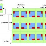
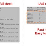
Accurate, comprehensive device recognition, connectivity extraction, netlist generation and, ultimately, circuit comparison becomes more complex with each new process generation. As the number of layers and layer derivations increases the complexity of devices, especially Layout Dependent… Read More
Conspiracy theories abound! The inside story of the Synopsys (SNPS) acquisition of Magma (LAVA) brings us back to the 1990’s tech boom with shady investment bankers and pump/dump schemes. After scanning my memory banks and digging around Silicon Valley for skeletons with a backhoe here is what I found out:
The Commission… Read More
Atrenta did an online survey of their users. Of course Atrenta’s users are not necessarily completely representative of the whole marketplace so it is unclear how the results would generalize for the bigger picture, your mileage may vary. About half the people were design engineers, a quarter CAD engineers and the rest … Read More
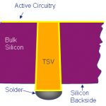
3D IC design and what has come to be known as 2½D IC design, with active die on a silicon interposer, require new approaches to verification since the through silicon vias (TSVs) and the fact that several different semiconductor processes may be involved create a new set of design challenges
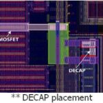
The power delivery network is a challenge… Read More
Low power techniquesby Paul McLellan on 12-08-2011 at 5:49 pmCategories: General
There was recently a forum discussion about the best low power techniques. Not surprisingly we didn’t come up with a new technique nobody had ever thought of but it was an interesting discussion.
First there are the techniques that by now have become standard. If anyone wants more details on these then two good resources are… Read More
Preventing electrical circuit failure is a growing concern for IC designers today. Certain types of failures such as electrostatic discharge (ESD) events, have well established best practices and design rules that circuit designers should be following. Other issues have emerged more recently, such as how to check circuits… Read More