You are currently viewing SemiWiki as a guest which gives you limited access to the site. To view blog comments and experience other SemiWiki features you must be a registered member. Registration is fast, simple, and absolutely free so please,
join our community today!
As a blogger I write weekly about the EDA industry and certainly our industry enables products like Smart Phones and Tablets to even exist, however if we really believed in these mobile devices then what should our web sites look like on a mobile device?
It’s a simple question, yet I first must define mobile-friendly before… Read More
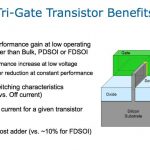
It was an honor to see DR. Chenming Huspeak and to learn more about FinFets, a technology he has championed since 1999. Chenming is considered an expert on the subject and is currently a TSMC Distinguished Professor of Microelectronics at University of California, Berkeley. Prior to that he was the Chief Technology Officer of TSMC.… Read More
D&R IP-SoC Days Santa Clara will be held on April 10, 2012 in Santa Clara, CA and if you plan to attend, just register here. IP market is a small world, and EDA a small market if you look at the generated revenue… but both are essential building blocks for the semiconductor industry. It was not clear back in 1995 that IP will become … Read More
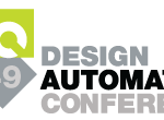
The technical program for DAC 2012 has an exceptional quality of technical papers, panels, special sessions, WACI (Wild and Crazy Ideas), WIP (Work In Progress), full day tutorials and user-track. The program is tailored for researchers and developers focused on electronic design automation (EDA) and embedded systems and … Read More
And no red and green glasses required.
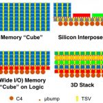
I remember the first time I heard about a Through Silicon Via (TSV), punching a hole through the entire wafer to make an electrical connection at the back, like we do all the time in printed circuit boards with through plated holes. I thought someone was trying one on and trying to make me look a fool.… Read More
EDPS Montereyby Paul McLellan on 03-17-2012 at 8:00 amCategories: EDA, Events
Every year in Monterey is a relatively small conference that looks at the design process, EDPS, the electronic design process symposium. I gave a keynote there a couple of years ago, but you don’t have to listen to me this time. The keynotes are from:
- 1st day: Misha Buric, CTO of Altera, talking about SoC FPGAs and other things
…
Read More
More Growth in EDAby Daniel Payne on 03-12-2012 at 6:53 pmCategories: Cliosoft, EDA
I love to read good news about growth in EDA especially when our industry has seen single-digit growth for several years now. What I read on March 8th from ClioSoft stated a 53% increase in bookings for 2011, now that’s what I call growth.
ClioSoft provides Hardware Configuration Management (HCM) software to EDA users typically… Read More
Next Wednesday is the Common Platform Technology Forum. “Common Platform” is a name that only a committee could have come up with, giving no clue as to what it actually is. As you probably know, there are various process clubs sharing the costs of technology development (TD) and one of them consists of IBM, Samsung and… Read More
Now that the dominant approach to building an SoC is to get IP from a number of sources and assemble it into a chip, the issue of IP quality is more and more critical. A chip won’t work if the IP doesn’t work, but it is quite difficult to verify this because the SoC design team is not intimately familiar with the IP blocks since… Read More
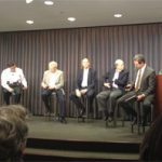
CEO Forecast Panelby Paul McLellan on 03-02-2012 at 2:40 pmCategories: EDA, Events
This year’s CEO forecast panel was held at Silicon Valley Bank. Bankers live better than verification engineers, as if you didn’t know, based on the quality of the wine they were serving compared to DVCon.
This year the panelists were Ed Cheng from Gradient, Lip-Bu, Aart and Wally (and if you don’t know who they… Read More