You are currently viewing SemiWiki as a guest which gives you limited access to the site. To view blog comments and experience other SemiWiki features you must be a registered member. Registration is fast, simple, and absolutely free so please,
join our community today!
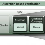
Assertion Synthesisby Paul McLellan on 08-28-2012 at 2:46 pmCategories: EDA
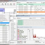
In June, Atrenta acquired NextOp, the leader in assertion synthesis. So what is it?
Depending on who you ask, verification is a huge fraction, 60-80%, of the cost of an SoC design, so obviously any technology that can reduce the cost of verification has a major impact on the overall cost and schedule of a design. At a high-level, verification… Read More
Increasingly the challenge with SoCs, especially for mobile, is not getting the performance high enough but doing so in a power-efficient manner. Handheld devices running multiple apps need high-speed processors that consume extremely low levels of power both in operating and standby modes. In the server farm, the limit is … Read More
Daniel Payne recently blogged some of the integration challenges facing Synopsys with their impending acquisition of SpringSoft. On my way back from San Diego last week I stopped by Tanner EDA to discuss an alternative tool flow for users who find themselves concerned about the Laker Custom Layout road map.
Design of the analog… Read More
At a dinner table a couple years ago, someone quietly shared their biggest worry in EDA. Not 2GHz, or quad core. Not 20nm, or 450mm. Not power, or timing closure. Call it The Rollover. It’s turned out to be the right worry.
Best brains spent inordinate hours designing and verifying a big, hairy, heavy breathing processor core to do … Read More
All semiconductor companies were caught up in ASIC in some way or another because of the basic economics. Semiconductor technology allowed medium sized designs to be done, and medium sized designs were pretty much all different. The technology didn’t yet allow whole systems to be put on a single chip. So semiconductor companies… Read More
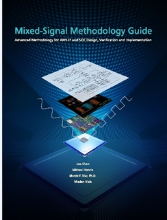
Almost every SoC has multiple analog blocks so AMS methodology is an important topic to our growing electronics industry. Authored by Jess Chen (Qualcomm), Michael Henrie (Cliosoft), Monte Mar (Boeing) and Mladen Nizic (Cadence), the book is subtitled: Advanced Methodology for AMS IP and SoC Design, Verification and Implementation… Read More
When I worked for virtual platform companies, one of the things that I used to tell prospective customers was that virtual prototypes were not some second-rate approach to software and hardware development to be dropped the moment real silicon was available, that in many ways they were better than the real hardware since they had… Read More
Synopsys announced their results today. With Magma rolled in (but not yet SpringSoft since that hasn’t technically closed) they had revenue of $443M up 15% from $387M last year. This means that they are all but a $1.75B company and a large part of the entire EDA industry (which I think of as being $5B or so, depending on just what… Read More
Cadence at 20nmby Paul McLellan on 08-21-2012 at 8:10 pmCategories: Cadence, EDA
Cadence has a new white paper out about the changes in IC design that are coming at 20nm. One thing is very clear: 20nm is not simply “more of the same”. All design, from basic standard cells up to huge SoCs has several new challenges to go along with all the old ones that we had at 45nm and 28nm.
I should emphasize that the paper… Read More
In the early 1980s the ideas and infrastructure for what would eventually be called ASIC started to come together. Semiconductor technology had reached the point that a useful number of transistors could be put onto a chip. But unlike earlier, when a chip only held a few transistors and thus could be used to create basic generic building… Read More