Have you notice how smart your automobile is getting? Watching the first round of NFL playoffs I lost count on the number of TV commercials showing cars weaving through tight construction zones (and Star Wars figures), big trucks parking in incredibly tight spaces, cars avoiding rear-end collisions and pedestrians, and even … Read More
Tag: dft
Finding Transistor-level Defects Inside of Standard Cells
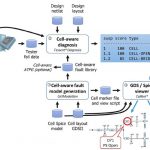
In the earliest days of IC design the engineering work was always done at the transistor-level, and then over time the abstraction level moved upward to gate-level, cell-level, RTL level, IP reuse, and high-level modeling abstractions. The higher levels of abstraction have allowed systems to be integrated into an SoC that can… Read More
Reducing the Cost of SoC Testing
Every year certain technology themes appear, like at ITC this year a big theme was how to reduce the cost of SoC testing. I spoke with Rob Knoth of Cadence by phone to hear more about this cost of test theme. Rob gave me an example of an SoC that takes 27 seconds on a tester, so at $0.04 per second in test costs amounts to $1.08 per part. If you… Read More
CEO Interview: Chouki Aktouf of Defacto Technologies
As a 30+ year semiconductor veteran I can tell you with 100% certainty that start-ups are the lifeblood of EDA. The mantra is “Innovate or Die!” and that is exactly what Defacto is doing. After more than 10 years of innovating in Design for Test at RTL, Defacto is now offering a complete EDA solution based on generic EDA… Read More
DFT Approaches for Giga-gate SoC Designs
In the early days of IC design there were arguments against using any extra transistors or gates for testability purposes, because that would be adding extra silicon area which in turn would drive up the costs of the chip and product. Today we are older and wiser, realizing that there are product pricing benefits to quickly test each… Read More
A Brief History of Defacto Technologies
In early 2000s, semiconductor design at RTL level was gaining momentum. The idea was to process more design steps such as insertion of test and other design structures upfront at the RTL level. The design optimization and verification were to be done at the RTL level to reduce long iterations through gate level design because changes… Read More
HW Emulator Apps Open Doors to Entirely New Uses
When the topic of hardware emulation comes up, thoughts of big iron customarily come to mind. However, hardware emulation has evolved significantly and now there are other important traits that distinguish the offerings in this area. For a very long period of time emulators provided primarily a method to accelerate gate level… Read More
Cadence Adds New Dimension to SoC Test Solution
It requires lateral thinking in bringing new innovation into conventional solutions to age-old hard problems. While the core logic design has evolved adding multiple functionalities onto a chip, now called SoC, the structural composition of DFT (Design for Testability) has remained more or less same based on XOR-based compression… Read More
Addressing Moore’s Law with the First Law of Real Estate: Location, location, location
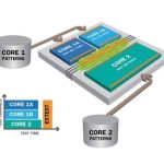
Design sizes and complexities have grown exponentially (it’s a Law!), and consequentially the task of silicon test has become proportionally more expensive. The cost of testing a device is proportional to the amount of test data that is applied, and therefore the time it takes, which in turn is proportional to both design size … Read More
An Universe of Formats for IP Validation
Although I knew about Crossfire’s capabilities for signing off quality of an IP before its integration into an SoC, there was much more to learn about this tool when I visited Fractal Technologies booth during this DAC. The complexity handled by this tool to qualify any type of IP for its integration into an SoC can be imagined by the… Read More


